Today, electronic systems have clock frequencies of a few hundred megahertz, and the front and back edges of the pulses used are in the sub-nanosecond range. The network interface transmits data rates of 100 Mbit/s and 155 and 622 Mbit/s (ATM-Asynchronous Transfer Mode). High quality video circuits are also used for sub-nanosecond pixel rates. These higher processing speeds represent an ongoing challenge in engineering.
One such challenge is radio frequency (RF) interference, which is caused by rapid changes in electromagnetic energy. The oscillation rate on the circuit becomes faster (rise/fall time), the voltage/current amplitude becomes larger, and the problem becomes more. Therefore, solving electromagnetic compatibility (EMC) is even more difficult today than before.
Before the two nodes of the circuit, the rapidly changing pulse current represents a so-called differential mode noise source, and the electromagnetic field around the circuit can be coupled to other components and invade the connection. The inductive or capacitively coupled noise is common mode interference. The RF interference currents are identical to each other and the system can be modeled as consisting of a noise source, a "damaged circuit" or "recipient" and a loop (usually a backplane). Several factors are used to describe the size of the interference:
â—The strength of the noise source
â— Interference current around the size of the area
â— rate of change
Thus, although there is a high probability of unwanted interference in the circuit, the noise is almost always co-modeled. Once the cable is plugged in between the input/output (I/O) connector and the chassis or ground plane, some RF voltages can cause a few milliamps of RF current to exceed the allowable emission level.
Noise coupling and propagationCommon mode noise is due to unreasonable design. Some typical reasons are the length of individual wires in different pairs, or the distance to the power plane or chassis. Another cause is component defects such as magnetic induction coils and transformers, capacitors and active devices (such as application specific integrated circuits (ASICs)).
Magnetic components, particularly so-called "core choke" type energy storage inductors, are used in power converters to always generate an electromagnetic field. The air gap in the magnetic circuit is equivalent to a large resistance in the series circuit, where more power is consumed. Thus, the core choke coil is wound on the ferrite rod, creating a strong electromagnetic field around the rod and having the strongest field strength near the electrode. In a switching power supply using a retrace structure, there must be a gap on the transformer with a strong magnetic field. The most suitable component in which the magnetic field is maintained is a spiral tube that distributes the electromagnetic field along the length of the die. This is one of the reasons why the magnetic element operating at high frequencies preferably has a spiral structure.
Inappropriate decoupling circuits often also become sources of interference. If the circuit requires a large pulse current and local decoupling does not guarantee a small capacitance or a very high internal resistance, the voltage generated by the power supply circuit drops. This is equivalent to ripple, or equivalent to a rapid change in voltage between terminals. Due to the stray capacitance of the package, interference can be coupled into other circuits, causing common mode problems.
When the common mode current contaminates the I/O interface circuit, the problem must be resolved before passing through the connector. Different applications suggest different ways to solve this problem. In the video circuit, where the I/O signals are single-ended and share the same common loop, to solve it, use a small LC filter to filter out the noise. In a low frequency serial interface network, some stray capacitance is sufficient to shunt noise onto the backplane. Differential drive interfaces, such as Ethernet, are typically coupled to the I/O area by a transformer that is coupled at the center tap on one or both sides of the transformer. These center taps are connected to the backplane via a high voltage capacitor to shunt common mode noise to the backplane so that the signal is not distorted.
Common mode noise in the I/O areaThere is no general way to solve the problem of all types of I/O interfaces. The main goal of the designers is to design the circuit, often ignoring some of the details that are considered simple. Some basic rules allow noise to be minimized before it reaches the connector:
1) Set the decoupling capacitor close to the load.
2) The pulse current of the rapidly changing front and rear edges should have a minimum loop size.
3) Keep high current devices (ie, drivers and ASICs) away from the I/O ports.
4) Determine signal integrity to minimize overshoot and undershoot, especially for critical signals (such as clocks, buses) for high currents.
5) Use local filtering, such as RF ferrite, to absorb RF interference.
6) Provide a low impedance bond to the backplane or the reference in the I/O area on the backplane.
RF noise and connectorsEven if engineers take many of the precautions listed above to reduce RF noise in the I/O area, there is no guarantee that these precautions will be successful enough to meet the launch requirements. Some noise is conducted interference, which is a common mode current flowing on the internal circuit board. This source of interference is between the backplane and the circuit. Thus, this RF current must flow through the path of the lowest impedance (between the backplane and the load signal line). If the connector does not exhibit a sufficiently low impedance (overlap with the backplane), this RF current flows through the stray capacitance. When this RF current flows through the cable, emission is inevitably generated (Fig. 1A).
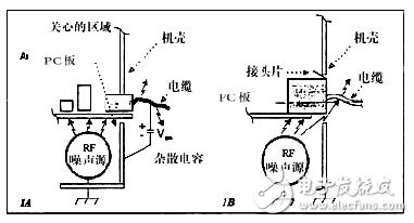
Another mechanism for injecting common mode current into the I/O region is the coupling of strong sources of interference nearby. Even some "shield" connectors are useless because the source of interference is in the vicinity of the connector, such as a PC environment. If there is a gap between the connector and the backplane, the RF voltage induced here can degrade EMC performance (Figure 1B).
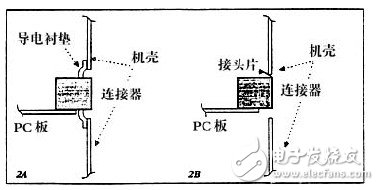
The method of shielding the connector is to add a finger spring or a spacer. The lap joint of the connector is filled between the connector and the casing. This method requires a pad (Figure 2A). Metal liners are preferred as long as the treatment is suitable, that is, as long as the surface is not contaminated, as long as the hand does not touch or damage the liner and as long as there is sufficient pressure to maintain good, low impedance contact.
Another method is to attach the connector to the connector or mount the connector on the chassis. At this time, the maximum contact surface is slightly smaller, and the size and elasticity of the tab should be strictly controlled. When installing the shielded connector, open it on the casing, and remove the oil on the side of the opening (Fig. 2B). Carefully make it. If the tolerance is not suitable, the connector will fall too deep in the casing, causing the overlap to be interrupted. Every EMC engineer knows that in an "excellent" system, this problem must meet the launch requirements and be checked in time on the production line. Untightened or bent gaskets that are installed in critical areas (such as the opening in which the connector is installed) will fail.
EMI connectors were selected for the following reasons;1) Conductive foamed plastic is extremely soft and can be placed around the entire connector. This eliminates the problems associated with another chassis and liner.
2) Mechanical engineers can install connectors within the tolerances that the system enclosure can accept.
3) The connector and the case achieve low impedance bonding to ensure good contact. The liner on the inside of the casing wall can be made of a softer material when it is required to be painted.
4) For designs requiring forced cooling, the liner preferably has another feature: the joint between the connector and the wall of the casing should be sealed to reduce air leakage. In dusty environments, the liner should be kept clean inside the system.
in conclusionThere are a variety of connectors on the market today that enable designers to get the best design for a particular interface.
About Key Accessories:
As we know ,everyone needs to use keys ,we use them in our household ,in our cars ,in our office,so we have many keys on hand ,in order to keep our keys well ,we may need keychains ,key rings and key covers for collecting keys in line ,and protecting our pockets,we don't want our life to be messy or lost our keys!
What we can do on Key Accessories?
Our factory have some common keychains to sell,and our main business is OEM ,we can help you to do Silicone Keychains/rings,PVC keychain,Silicone Wristband keychains,Silicone Key Cover,if you have your ideal designs ,please tell us ,we can help you to achieve by your requirements!
Some Key Accessories photos for your ref.


Key Accessories
Key Accessories,Custom Made Keychains,Custom Pvc Keychain,Silicone Key Sleeve
OK Silicone Gift Co., Ltd. , https://www.oemsiliconegift.com