The scale of modern hardware design is gradually increasing, and the function of a single program is more and more complicated. When multiple complex programs are integrated into one FPGA, the FPGA control module is caused by the conflict of data channels and occupied resources of each program. The structure is bloated, affecting the efficiency of the entire system.
The multi-configuration of the FPGA can effectively simplify the design of the control structure, and at the same time, the FPGA device with less logic resources can be used to implement a program that requires a lot of resources. Based on the Virtex5 series development board and configuration memory SPI FLASH, the multiple configurations are analyzed from two aspects of hardware circuit and software design. The specific steps of multiple configuration implementation are given, which has certain reference value for implementing complex hardware design engineering.
0 Preface
The scale of modern hardware programming is getting bigger and bigger, and the functions are more and more complicated. When multiple applications are implemented on one hardware platform at the same time, the resource usage and data path of each program may conflict, which increases the complexity of control circuit design. The degree has increased the workload and development difficulty for developers. With multiple configurations, multiple applications can be loaded into the FPGA as needed, which not only simplifies the circuit design, but also makes the system more flexible. The multi-configuration features of FPGAs allow users under certain conditions to select FPGAs with few on-chip resources to implement functions that require many resources for FPGAs, which greatly reduces development costs and increases FPGA utilization.
Xilinx's Virtex5 series of FPGAs have multiple configuration features, allowing users to choose one of the multiple bit files stored in the FLASH to convert the system functions according to the needs of different moments without power-down restart. .
1 overall design
After the FPGA completes the power-on automatic loading of the initialized bit stream, the FPGA can be reconfigured by automatically triggering a new bit stream from the address specified by the external configuration memory (SPI FLASH) by triggering multiple startup events inside the FPGA. Multiple configurations of FPGAs can be implemented in a variety of ways. This paper uses the state machine coding method based on the ICAP core. By calling Xilinx's own ICAP core, the authoring state machine continuously configures the ICAP core according to a certain instruction flow, and can control the FPGA reconfiguration. This method can add a lot of comments in the source code, so that later developers can clearly understand the ICAP kernel instruction stream sequence, and multiple configuration address calculation methods, which is a simple and practical implementation method.
1.1 hardware circuit
The multi-configuration hardware mainly includes the FPGA board and the FLASH chip that stores the configuration files. The FPGA uses the ML507 from the XILINX Virtex-5 family, which adds dedicated internal loading logic for multiple FPGA configurations. The FLASH chip uses XILINX's SPI FLASH chip M25P32, which has a storage space of 32 Mb. The number of storage files is related to the file size and the FPGA chip used. To implement multiple configurations, first connect the FPGA and external configuration memory to the mode in which the configuration file is loaded from SPI FLASH. The block diagram of the configuration circuit hardware connection is shown in Figure 1.
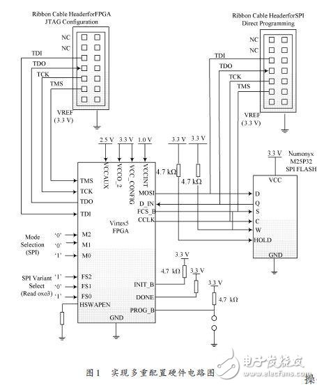
In FPGA configuration mode, M2, M1, M0 are 0, 0, 1. This configuration mode corresponds to boundary scan plus pull. In this mode, all I/O of the FPGA is valid only during configuration. After the configuration is completed, the unused I/O will be floated [5]. M2, M1, M0 The three selection switches correspond to the 4, 5, 6 bits in the SW3 switch on the ML507 development board, before the FPGA is powered on. Turn the above switch to the 0,0,1 state.
1.2 software design
From the perspective of software design, FPGA multi-configuration can be divided into two parts. The first part is the user-developed program. This part includes the functions that the user wants to implement on the FPGA. It also includes the clock signal for the heavy-duty module and the trigger signal. The trigger signal is received by the user program to write the serial communication protocol stack. The number transmitted by the PC is used as a trigger signal. The second part is the FPGA reload configuration module. The FPGA multi-configuration first needs to call the ICAP core. When the trigger condition is met, the ICAP core is assigned by the state machine coding. The software structure diagram of FPGA multiple configuration is shown in Figure 2.
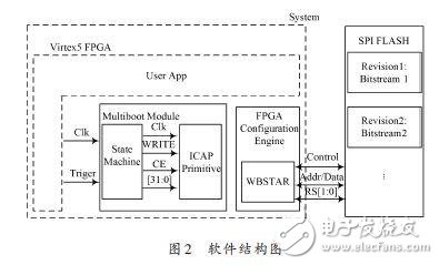
The overloaded module first calls the ICAP core. The ICAP primitive is called in Xilinx's compiling software ISE. The calling path is Edit→LanguageTemplates, VHDL/Verilog→Device PrimiTIve InstanTIa-TIon→Virtex5FPGA→Config/BSCAN Components→In-ternal Config Access Por(t ICAP_VIRTEX5).
The ICAP_VIRTEX5 call interface is as follows:
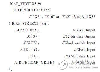
The ICAP core supports three data bandwidth modes: X8, X16, and X32. The output of the ICAP core is not used during the entire FPGA reconfiguration process. Therefore, the values ​​of the BUSY and O signals are not concerned with the state machine control program of the reload module, and they may not be assigned values. When the user program uses the interface, it only needs to continuously assign values ​​to the CE, CLK, I, and WRITE signals to send commands.
After the ICAP core interface is invoked, the state machine is implemented by Verilog encoding. The IPROG instruction is sent to the ICAP core through the state machine. After receiving these instructions, the ICAP core automatically loads the configuration file according to the specified address.
In the event of a power outage, the emergency exit light displaying the exit sign must remain lit for an emergency period of 90 minutes and must remain lit continuously in working condition. Specially designed plastic and acrylic materials are lightweight, ABS material is strong, insulating, and not conductive. The letters "EXIT" can be printed on the transparent acrylic sheet and can be customized in green or red. Easy to install, simple to operate, can be hung on the wall or hung from the ceiling. The Emergency Exit Sign lamp suitable for different commercial buildings or public places such as hospitals, schools, subways, train stations, etc.

Fire Emergency Signs,Weatherproof Exit Sign,Illuminated Fire Exit Signs,Battery Operated Emergency Lights
Jiangmen City Pengjiang District Qihui Lighting Electrical Appliances Co., Ltd , https://www.qihuilights.com