1 Overview
With the rapid development of image processing technology, image acquisition and processing systems are becoming more and more widely used in improving the automation level of industrial production. Combining the needs of front-end image processing and image data transmission in the actual system, this paper makes full use of the flexibility of ARM and the parallelism of FPGA to design a high-speed image data acquisition and transmission system based on ARM+FPGA. The selected ARM architecture is a 32-bit embedded RISC microprocessor architecture with a rich instruction set and flexible programming. FPGAs have great advantages in speed and parallel computing, and are suitable for real-time image processing. Requirements; and high-speed remote transmission of image data between the acquisition board and the host computer through the Gigabit Ethernet interface.
2. Hardware design
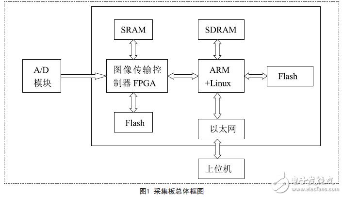
2.1 Overall system design
The ARM chip used in this design is Samsung's S3C2440A, and the FPGA chip is the Spartan series S3C500E chip produced by Xilinx. The system consists of Gigabit Ethernet control chip AX88180, Gigabit PHY chip 88E1111, memory, embedded Linux, network. Drivers, etc. (as shown in Figure 1).
The main control chip S3C2440A of this design is a 16/32-bit RISC microprocessor based on ARM920T core. It adopts 0.13um CMOS standard macro unit and memory unit and runs at up to 500MHz. ARM920T implements MMU, AMBA BUS and Harvard cache. Architecture. This structure has a separate 16KB instruction cache and 16KB data cache. Each consists of rows of 8 words long. By providing a complete set of general-purpose system peripherals, the S3C2440A reduces overall system cost and eliminates the need to configure additional components. It is targeted at handheld devices and cost-effective, low-power applications with a rich set of on-chip resources.
The FPGA chip S3C500E is mainly used for image sensor control, image data buffering and peripheral chip timing generation. It realizes data acquisition by controlling A/D, and saves it to SRAM, decodes the ARM read/write signal to read the target data back to ARM and transmit it to the host computer.
The ARM chip S3C2440A is responsible for the control of the entire system. It reads and writes the address on the bus to transfer instructions and data to control all actions of the FPGA [1-2]. The embedded Linux kernel is responsible for the management of system tasks and integrates the TCP/IP protocol to facilitate network control functions.
S3C2440A and AX88180 are connected by bus, which is the main body of communication control. The S3C2440A implements the internal register programming of the AX88180 through the network driver, as well as the transmission and reception of Ethernet data, thereby completing the data transmission between the network and the system.
The AX88180 and 88E1111 are interconnected by the RGMII interface, which is responsible for the implementation of the underlying protocol for data transfer.
2.2 Data Acquisition Interface Design
The difficulty of system design lies in the design of the data acquisition interface, which is the channel for data transmission, and also the bridge connecting the front and rear ends of the system. The system uses S3C2440A and S3C500E to jointly realize high-speed data acquisition.
Direct Memory Access (DMA), as a CPU-independent background batch data transmission technology, has been widely used in the field of data acquisition due to its fast and efficient features. In this design, the S3C2440A uses an external DMA method to collect the internal storage data of the FPGA. The interface signal connection is shown in Figure 2.
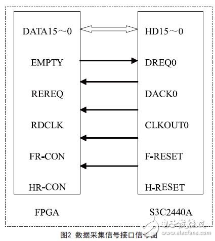
The FPGA part of the interface design mainly consists of an asynchronous FIFO module, a reset module and a data buffer module. The asynchronous FIFO module mainly solves the problem that the image output data frequency and the data acquisition frequency do not match. The asynchronous FIFO width adopted by the system is 8 bits and the depth is 2048. The reset module realizes the reset control of the system FIFO under the action of the control signal.
The system uses DMA channel 0 to acquire image data.
In-ear Wired Earphones, they are small and comfortable and simple, fit in just about any pocket,and they provide great sound that literally goes straight into your ears,bring it on your next commute or run, or simply enjoy it in the comfort of your time.
In-ear Wired Earphones
Earbuds With Removable Cable,Earphones With Replaceable Cabl,Stereo In-Ear Earphones,In-Ear Wired Headphones
Dongguang Vowsound Electronics Co., Ltd. , https://www.vowsound.com