Abstract: This paper presents a component-based structure for an infrared video acquisition system utilizing FPGA technology. It details the implementation of each functional module, including HDL code, SignalTap II waveforms, and Quartus II top-level schematics. A prototype circuit board was developed for debugging, enabling real-time infrared image display through VGA output. The results demonstrate that the system effectively leverages the advantages of FPGA technology, offering excellent scalability, flexible control, and a short development cycle.
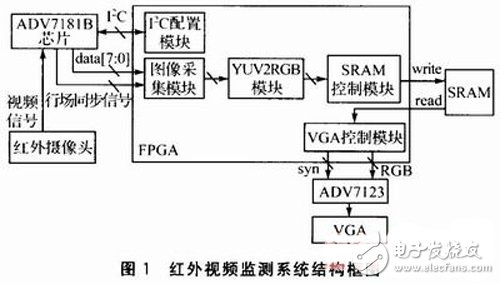
1 System ArchitectureThe FPGA-based infrared video monitoring system comprises five key modules: I2C configuration, image acquisition, YUV to RGB conversion, SRAM control, and VGA control. The I2C configuration module sets up the ADV7181B chip via the I2C bus. Once configured, the ADV7181B generates the necessary line sync signal and converts the composite video input from the infrared camera into a standard NTSC/PAL format for the image acquisition module. This module extracts valid YUV (BT656) data from the video stream. The YUV2RGB module then converts this data into RGB format for VGA display. The VGA control module manages synchronization signals and reads data from the SRAM to drive the D/A converter (ADV7123). Figure 1 illustrates the overall block diagram of the system.
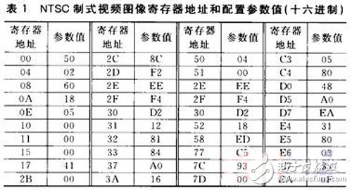
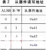
The ADV7181B is a widely used video decoder from Analog Devices. It automatically detects the input composite video signal and can be configured via the I2C bus to select the output mode, such as NTSC or PAL. This paper provides the configuration register addresses and values for NTSC output. These are listed in Table 1. The ADV7181B operates as a slave device on the I2C bus, with different read/write addresses depending on the ALSB pin configuration. The system grounds the ALSB pin and sets the write address to 0x40, as shown in Table 2.
NTSC video outputs alternate between even and odd fields. The timing relationship between the data signal and the line sync signal is illustrated in Figure 2. Each field contains 253 active lines. This paper focuses on capturing the even field for transmission. BT.656 defines a parallel interface for YCbCr 4:2:2 format, where each pixel occupies two bytes in the order CbYCrY. The module extracts one set of CbYCr every two pixels and sends it through a shift register to the YUV2RGB module. This reduces the effective pixel count from 720×525 to 360×253.
The SAV (Start of Active Video) and EAV (End of Active Video) markers help identify the start and end of image data within each line. For example, the odd field starts with 0xC7 and ends with 0xDA, while the even field begins with 0x80 and ends with 0x9D. These codes are based on the detected sequence "FF, 00, 00.xy" from the ADV7181B output. The meaning of these codes is detailed in Table 3, which includes information about field type, video validity, and line synchronization.
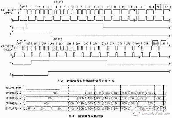
Figure 3 shows the timing of image data acquisition using SignalTap II. During the hcTIve_even high period, the image data is captured. The yuvdin signal represents the 8-bit parallel output from the ADV7181B. When the sequence "FF 00 00 ε0" is detected, the system starts collecting the even field's effective pixels. The extracted data from registers reg1, reg2, and reg3 are sent to the RGB conversion module for further processing.
2.3 YUV to RGB Conversion ModuleTo display images on a VGA monitor, the YUV data must be converted to RGB format. The conversion formulas are as follows:
R = 1.164(Y - 16) + 1.596(Cr - 128)
G = 1.164(Y - 16) - 0.813(Cr - 128) - 0.392(Cb - 128)
B = 1.164(Y - 16) + 2.017(Cb - 128)
Floating-point calculations are resource-intensive on FPGAs. To optimize performance, a lookup table is used. The coefficients from the equations are precomputed and stored in the table. For example, multiplying equation (1) by 2 simplifies the calculation. The lookup table is shown in Figure 5. By using this method, the R component is calculated as (a + b - 446)/2 if (a + b) > 446, otherwise it is zero. Similar logic applies to the G and B components.
Since the SRAM data line is 16 bits, the RGB components (R: 5 bits, G: 6 bits, B: 5 bits) are written to the SRAM. When RGB_wrdata is non-zero, the data is stored, achieving a resolution conversion from 720×525 to 360×250. This ensures efficient memory usage and real-time image display through VGA output.
Heat Shrinkable Tube,Shrink Tube,Heat Shrink Sleeve,Clear Heat Shrink Tubing
Shenzhen Huiyunhai Tech.Co., Ltd. , https://www.cablesleevefactory.com