Abstract: This paper presents a component-based structure for an infrared video acquisition system utilizing FPGA technology. It details the implementation of each functional module, including HDL code, SignalTap II waveform analysis, and Quartus II top-level schematics. A prototype circuit board was designed for testing, and the system successfully displays real-time infrared images via VGA output. The results demonstrate that the system effectively leverages the advantages of FPGA technology, offering excellent scalability, flexible control, and a short development cycle.
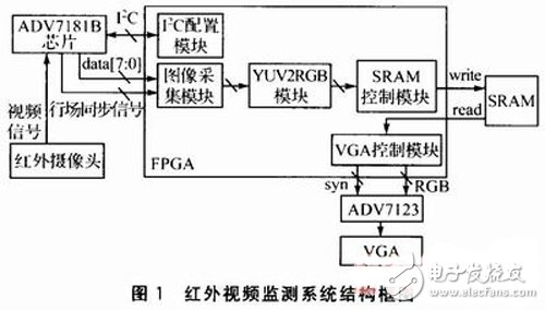
1 System ArchitectureThe FPGA-based infrared video monitoring system consists of five key modules: the I2C configuration module, image acquisition module, YUV2RGB conversion module, SRAM control module, and VGA control module. The I2C configuration module is responsible for setting up the ADV7181B video decoder chip. Once configured, the ADV7181B generates the necessary line synchronization signal and converts the composite video input from the infrared camera into a standard NTSC/PAL format. The image acquisition module extracts the valid YUV (BT656) data from the video stream, while the YUV2RGB module converts this data into RGB format suitable for VGA display. The SRAM control module manages the read and write operations of the image data, and the VGA control module generates the required synchronization signals and controls the D/A conversion process using the ADV7123 chip. A block diagram of the system is shown in Figure 1.
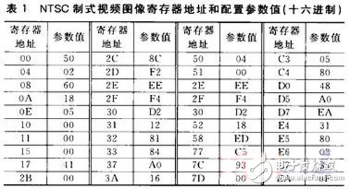
The ADV7181B is a commonly used video decoder chip from Analog Devices. It can automatically detect the input composite video signal and configure the output mode (NTSC or PAL) through the I2C bus. This paper focuses on the NTSC configuration, providing the corresponding register addresses and values. Table 1 lists the register addresses and configuration parameters for NTSC video output.
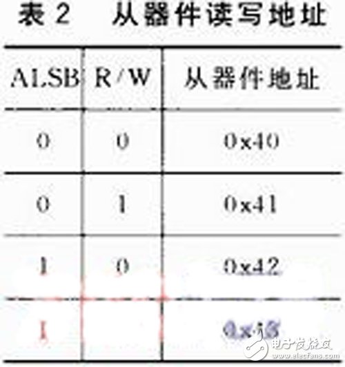
As a slave device on the I2C bus, the ADV7181B has different addresses based on the state of the ALSB pin. The read and write addresses are summarized in Table 2. In this design, the ALSB pin is grounded, setting the write address to 0x40. All values are expressed in hexadecimal.
The default output of the NTSC video alternates between even and odd fields. The timing relationship between the data signal and the line sync signal is illustrated in Figure 2. Each field contains 253 active lines. This paper processes the even field for display. The BT.656 standard defines a parallel hardware interface, where the video data is transmitted in the form of YCbCr 4:2:2. Each line of image data has 720 effective pixels, with each pixel occupying two bytes in the format CbYCrYCbYCrY. By processing every two pixels, the system obtains one set of CbYCr and outputs it as CbYCrY. These data are then sent to the YUV2RGB module through a shift register, compressing the effective pixels to 360 per line. The module collects 720×525 image data, but only 360×253 effective pixels are available for transmission.
The start and end of each line (SAV/EAV) and the frame position are determined based on the BT.656 format, specifically by detecting the sequence "FF, 00, 00.xy" from the ADV7181B output. The odd field starts with xy = 0xC7 and ends with xy = 0xDA, while the even field begins with xy = 0x80 and ends with xy = 0x9D. The meaning of these values is detailed in Table 3. The highest bit (bit 7) indicates whether the data is the same, F=0 represents the even field, F=1 the odd field, V=0 means active video, V=1 no active video, H=0 is SAV, and H=1 is EAV. The lower four bits are protection signals.
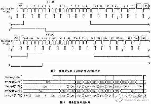
Figure 3 shows the timing of image data acquisition captured using SignalTap II. The hcTIve_even high period corresponds to the effective image data acquisition phase, and yuvdin represents the 8-bit parallel image data from the ADV7181B. When the sequence "FF 00 00 ε0" is detected, the system starts collecting the effective pixels of the even field. The black lines labeled reg1, reg2, and reg3 represent the extracted image data for the three channels, which are then sent to the RGB conversion module.
2.3 YUV2RGB Conversion ModuleTo display the image on a VGA monitor, the YCrCb data must be converted to RGB format. The conversion formulas are as follows:
R = 1.164(Y - 16) + 1.596(Cr - 128)
G = 1.164(Y - 16) - 0.813(Cr - 128) - 0.392(Cb - 128)
B = 1.164(Y - 16) + 2.017(Cb - 128)
Floating-point calculations require significant FPGA resources, which can impact system performance. To reduce computational complexity, the system uses a lookup table approach. Five different coefficient components from the equations are precomputed and stored in the lookup table. For further simplification, equation (1) is multiplied by 2, resulting in the simplified formula: 2R = a + b - 446, where a = 2 × 1.164Y and b = 2 × 1.596Cr. If (a + b) > 446, R = (a + b - 446)/2; otherwise, R = 0. Similar logic applies to the G and B components, completing the YCrCb to RGB conversion. Since the SRAM data line is 16 bits, each of the three 8-bit RGB components (R: 5 bits, G: 6 bits, B: 5 bits) is written to the SRAM. When RGB_wrdata is non-zero, the image data is stored in the SRAM, achieving a resolution conversion from 720×525 to 360×250.
Open Type Braided Sleeve,Braided Sleeving,Braided Cable Sleeve,Braided Sheath
Shenzhen Huiyunhai Tech.Co., Ltd. , https://www.cablesleevefactory.com