The audio signal detector introduced here is the audio signal injection / tracker. It can be used to overhaul audio equipment such as video disc players, radios, amplifiers, recorders, CD players, VCDs, DVD players, as well as overhaul the audio circuits of televisions, home theaters and other equipment. The audio signal injection / tracker is a relatively simple and commonly used instrument. It is actually a combination of the following two instruments.
One is the signal injector. Through the probes on the front of the instrument, audio signals are injected into all levels of the circuit under repair to determine the fault.
The second is the signal tracker. Through the probe at the front of the instrument, the audio signal is searched from all levels of the circuit under repair to determine the fault.
The following analyzes the circuit diagram of the audio signal injection / tracker.
1. The whole machine circuit analyzes the audio signal injection / tracker circuit as shown below.
Since the instrument has two functions of "signal injection" and "signal tracking", we can first determine that Sl is a function selection switch. When Sl is placed in the "xJ" file, the circuit forms a signal tracker; when Sl When placed in the "ZR" file, the circuit constitutes a signal injector.
In the figure below, Sl points to the "XJ" file, and the circuit forms a signal tracker.
We know that the function of the signal tracer is to amplify and play the audio signal of the detected circuit. Therefore, the probe (x) on the left of the circuit diagram is the signal input terminal, and the speaker (BL) on the right of the circuit diagram is the final load. The processing flow direction is from left to right. The battery (GB) as the power supply of the whole machine is on the right side of the circuit diagram, so the direction of the DC power supply circuit is from right to left.
The following sequentially analyzes the signal tracer and signal injector circuits.
(1) Signal tracker
From the picture below
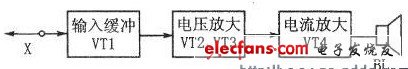
(Sl points to "xJ") It can be seen that the main components of the signal tracer circuit are 4 transistors. With these 4 transistors as the core, the circuit diagram can be divided into 3 units, from left to right in order: â‘ input buffer unit with the transistor VT1 as the core; â‘¡voltage amplifying unit with the transistors VT2 and VT3 as the core; â‘¢ Transistor VT4 is the core current amplification unit. The above unit circuit constitutes the overall circuit of the audio signal tracker, the right figure is its block diagram. The working principle of the circuit is: the weak audio signal taken out by the probe X from the detected circuit is buffered by VT1 and then sent to VT2 and VT3 for voltage amplification, and then amplified by VT4 current to drive the speaker BL to sound. Below we analyze each unit circuit of the circuit diagram from left to right.
1) Analysis of the input buffer unit circuit. Transistors VT1 and R3, R4, etc. constitute an emitter follower, the signal is input from the base of VT1 and output from its emitter. C3 and C4 are DC blocking capacitors at the input and output, respectively. The emitter follower is actually a common collector amplifier circuit. The output signal is taken out from the emitter resistor R4. At the same time, R4 is connected in series in the input signal loop to negatively feedback the output voltage to the input. A voltage series feedback amplifier with a feedback coefficient of 1. Due to the effect of deep negative feedback, the emitter follower has:
â‘ Very high input impedance; â‘¡ Very low output impedance; â‘¢ Voltage gain is slightly less than 1, the output voltage is in phase with the input voltage; â‘£ Current gain is equal to the transistor current amplification factor and other characteristics.
As the input stage of the whole instrument, the emitter follower has a very high input impedance, which has minimal impact on the detected circuit, and plays a role of buffer isolation between the detected circuit and the amplifier circuit. R3 is a bias resistor that provides base bias current for VT1.
2) Circuit analysis of voltage amplification unit. Transistors VT2, VT3, etc. constitute a dual-tube voltage amplifier, which amplifies the detected signal sent from the input buffer stage. The signal output by the emitter follower VT1 is coupled to the base of VT2 by C4. After being amplified by the two-tube amplifier, it is output from the collector of VT3 and coupled to the subsequent circuit by C6.
The dual-tube amplifier has the characteristics of large voltage gain and high operating point stability. The two-tube amplifier is formed by directly coupling two-stage common-emitter amplifiers, and the total voltage gain is equal to the product of the two-stage voltage gain. The base bias voltage of VT2 is not taken from the power supply voltage, but is taken from the emitter voltage of VT3 (voltage drop on R9) through R7, which forms a DC negative feedback to stabilize the operating point of the circuit. For example: when the collector current of VT2 rises for some reason, the collector current of VT3 decreases due to direct coupling, and the voltage drop on R9 also drops. The feedback to the base of VT2 through R7 forces the collector current of VT2 to fall, thus maintaining Working point stability. Adjusting R7 can change the working point of VT2 and VT3. R5 and R8 are the collector resistance of VT2 and VT3 respectively. R6 is the emitter resistance of VT2, which can generate negative current feedback to further stabilize the operating point of this stage.
It can show your brand in a different way. The meta part is available
in several colors, such as white ,red,black ,blue,green and sliver.It
will be lighted when plug in computer . There are also multi-color LEDs
are available.
Note: No MOQ limited and free make sample with LOGO .contact with us for more.
Crystal USB Flash Drive,Crystal USB Stick,Wholesale USB Flash Drive,Crystal Flash Drive
Custom Usb Gift company limited , https://www.customusbgift.com