Summary
The use of PCI Express for computing applications (servers, networking, laptops, etc.) is quite popular over time and is used in smaller, battery-powered devices (phones, tablets, watches, etc.) It is becoming more extensive. Because of the increased data traffic between devices in a computing application environment, resulting in greater power requirements, it is for this reason that designers are looking for ways to reduce their SOC power during low-intensity or idle periods. Smaller, battery powered devices are often in idle and deep sleep mode, but for this type of deep power save mode, the cost is that the recovery time is longer when switching back to normal operating mode.
For designers using PCI Express, the integration of PCI Express IP into their SOC has a positive impact on the power of their target applications, in addition to the energy-saving technologies provided by the protocol, as well as advanced power management techniques. You can control power consumption. The use of clock gating technology can handle dynamic power issues, but has no effect on static power consumption. Power gating technology is ideal for maximum power savings because it reduces the need for larger static power due to reduced feature size. In deep power-saving mode, power-gated PCI Express IP typically requires PCI Express link retraining or reconfiguration and will extend recovery time, which is undesirable in many situations, so it is a major challenge .
In this article, PCI Express IP is used as an example to describe three energy-saving technologies and how designers can use the power management features of protocols and design tools to provide energy-efficient SoCs for devices that require fast recovery.
1. Clock Gating Technology: Comprehensive Tools Modern synthesis tools provide several clock power management techniques, such as traditional clock gating and self-gating. In traditional clock gating, the synthesis tool looks for conditions and combines them to form a clock enable (EN) that shuts down the clock-to-trigger path. Here is an integrated clock gating (ICG) unit that uses EN to turn off the clocks of a series of flip-flops, as shown in Figure 1. For self-gating techniques, if the input to the flip-flop is unchanged, the trigger clock is turned off; the output of the flip-flop is XORed with the input and used as the clock enable (EN) in the ICG.
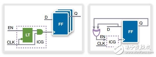
Figure 1. Traditional clock gating (left) and self-gating (right)
This strategy led to an energy-efficient CE, but the area increased slightly due to additional logic overhead. Synthetic tools typically use self-gating after plugging in traditional clock gates to enhance CE and further reduce energy consumption for area trade-offs. The automated method can be evaluated and optimized using power analysis tools that can communicate the efficiency of existing clock gates and reveal opportunities for further insertion into the clock gate. For several use cases, this type of report can be used to further optimize clock gate insertion.
Optimized traditional clock gating and PCI Express IP can achieve at least 40% energy savings and reduce the area on the 28nm technology node by approximately 9%.
The self-gating strategy after the traditional clock gate is inserted can reduce the energy consumption by at least 5% and increase the area by about 1%. At the 16nm FinFET (16FF) technology node, the integrated tool clock gating (conventional clock gating + self-gating) achieves 25% energy savings. figure 2.
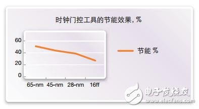
Figure 2. Energy savings from the clock gating tool
2. Clock Gating Technology: PCI Express IP
While tool plug-in clocking technology can significantly reduce power consumption, they do not fully consider the design level. The CE obtained from the design aspect acts only on the flip-flop, and only gates the clock at the clock input of each flip-flop, as shown in Figure 3. There is a complaint in this regard that the tool plug-in clock gating is too "subtle" and does not consider passing through the entire hierarchy of clock trees.
The clock tree includes clock drivers and clock gating units distributed throughout the design, and switching is independent of drive logic. For highly complex designs, the clock tree consumes at least 25% of standby power. Turning off the clock at the root of the hierarchy reduces power consumption because of clock tree switching, a design decision that requires architectural considerations.
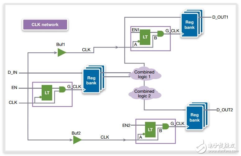
Figure 3. Typical design after clock pulse gate insertion
As an example, consider the PCI Express IP design and the ARM® AMBA® interface and three clock domains, as shown in Figure 4. The AMBA master receives the PCI Express request and converts it to an AMBA transaction, which is sent to the application layer on the AMBA master clock. The AMBA slave device processes the AMBA transaction from the application layer and converts it to a PCI Express request on the AMBA slave clock. The remaining blocks perform specific PCI Express functions to process round-trip requests on the core clock or reference clock line.
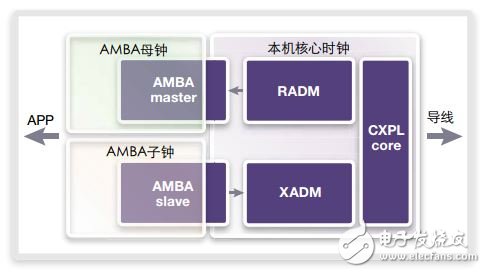
Figure 4. PCI Express IP and 3 clock domains
There are multiple scenarios with AMBA master/slave idle, completely independent of the PCI Express link state:
1. For inbound requests from the line, the local core clock domain and the AMBA master clock domain are required to keep running while turning off the AMBA slave clock.
2. For outbound requests from the application layer, the AMBA slave clock and the local core clock domain are required to be running and the AMBA master clock is turned off.
3. For inbound/outbound requests that do not require logical intervention, only the local core clock domain is required, and at the same time, the AMBA master and slave clocks can be turned off.
Clock gating in the fabric module does not need to comply with the link power management state of PCI Express. If there are no pending requests in a particular direction, the clock to the standby fabric module can be disconnected. In the AMBA master-slave clock block, the clock can be turned off at the root, reducing the power consumed by a particular clock tree. For scenario 3, implementing the same approach in PCI Express IP can save at least 10% power and increase standby processing efficiency by at least 10%.
In Table 1, the power consumption at full load communication and standby state is introduced, with and without structured clock gating.

Table 1. Power Comparison of Structured Clock Gating Implementations
3. Clock Gating and Power Gating Technology: PCI Express Protocol
The PCI Express protocol allows for power optimization by means of finer link states, L0, L1 (sub-state) and L2/L3, which are defined as power management states according to the specification. To exit the L2 and L3 states, power is restored and the link is trained again, resulting in longer recovery times. At L0 and L1 (sub-states), clock gating techniques are employed to minimize recovery time. Consider the PCI Express IP design introduced in Section 2. Under L0, the AMBA master-slave clock can be selected, depending on the path direction under L0, and the reference clock is not required in the L1 sub-state. Therefore, even if the local core clock can be turned off without stopping the phase-locked loop (PLL), the PLL can generate a core clock to avoid delay when restarting the PLL. The power consumption in this case is the lowest of all clock gating techniques, with leakage power only in digital and analog circuits.
If you can tolerate up to 5 times the recovery time, you can disconnect the PLL and transmitter/receiver in the L1.1 substate, up to 97.5 compared to the L1.1 substate with only clock gating. % energy saving effect. If it can tolerate up to 15 times recovery time, even the common mode voltage can be disconnected in the L1.2 substate, reducing the power consumption to 0.05%.
PCI Express provides message-based system power processing assistance techniques such as Delay Allowed Notification (LTR) and Optimized Buffer Clear/Complete (OBFF). With the LTR, the maximum delay allowed by the downstream device can be passed upstream, enabling the host software to understand the recovery time required for seamless link operation. With OBFF, the host software can transfer system status to downstream devices with master line control capabilities, use them to optimize transmission schedules, and make the system work longer in power-saving mode. For example, if the system is in a low power state, there will be a delay in the routine DMA transfer. For information collected from the LTR, it can be used to determine how much to extend the standby time in order to allow for a higher seemingly feasible energy savings.
Conclusion Power management is especially important for devices in sporadic communication and standby processes with expected fast recovery times. Tool-based design-related and protocol-related clock gating techniques enable maximum energy savings for interface IP designs such as PCI Express. Clock gating solutions achieve excellent results when near-zero recovery times are required. Maximum power savings and faster recovery times are achieved by avoiding PCI Express link retraining and reconfiguration.
For Synopsys' DesignWare IP solution for PCI Express technology, it takes advantage of tool-based clock gate insertion technology.
Includes structured clock gating blocks that are dependent and independent of PCI Express link power state;
Support PCI Express clock power management in L1 substate;
Provides power gating solutions, as well as power island and register retention methods for L1.2 substates (avoiding link retraining), support for power management assistance features such as delay tolerant notification (LTR) and optimized buffer clearing/filling ( OBFF).
Supports all PCI Express power management features, including longer recovery times, such as dynamic uplink and downlink configuration and L2/L3 power gating.
Using PCI Express IP that supports these features helps designers deliver energy-efficient SoCs.
Https://Company/PublicaTIons/DWTB/Pages/dwtb-L1-substat...
The design of the terminal blocks with clamping yoke connections which has contact pressure and has with self-locking function.Providing test type,knife Disconnect,fuse type terminal blocks etc.The cross-sectional is 0.5-35mm².
Marker Carrier For Terminal,Screw Connection End Stopper,Terminal Block End Stopper,Terminal Connection End Clip
Wonke Electric CO.,Ltd. , https://www.wkdq-electric.com