
Intel's semiconductor frontier technology reserves
What are the killers that will win the future?
Exclusive secret, just know IN


Intel Technology and Manufacturing Frontier Research Program
Intel's Components Research team fund sand works with universities and academic research consortia on forward-looking research topics such as Spintronics, and also on the understanding of fundamental science which is the basis of these forward-looking research.
Intel's cutting-edge research department sponsors a number of universities, colleges, and academic institutions to work on a variety of cutting-edge research topics, such as spintronics and the underlying science of these cutting-edge research.
Mark T. Bohr, Director of Process Architecture and Integration, Intel Senior Fellow, Technology and Manufacturing Division
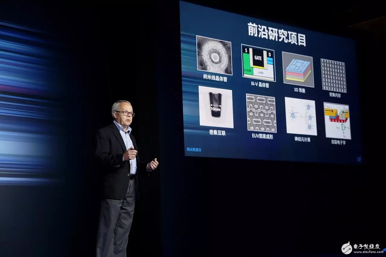
Interpretation of Intel's cutting-edge research projects
1
Nanowire transistors are being explored as a future option because the nanowire structure provides improved channel electrostatics that can enable further transistor gate length scaling.
Nanowire transistors are considered an option for future technologies because the structure of the nanowires provides improved channel statics, further miniaturizing the transistor gate length.
2Silicon has always been the material used in MOSFET channels, but III-V materials such as GaAs and InP have improved carrier mobility that can provide higher performance or the ability to operate transistors at lower voltage for lower active power.
Silicon is a commonly used material in MOSFET channels, but III-V materials such as gallium arsenide and indium phosphide improve carrier mobility, providing higher performance or lower voltages and lower Run the transistor under active power.
33D stacking of silicon die can provide system integration opportunities to mix different technologies into a small form factor.
The 3D stacking of silicon wafers has the opportunity to integrate the system to mix different technologies into one small place.
4A variety of dense memory options, including volatile and non-volatile memory, are being explored and developed.
A variety of different high-density memory options, including volatile and non-volatile storage technologies, are being explored and developed.
5Scaling interconnects is just as important as scaling transistors on advanced process technologies. Novel materials and patterning techniques are being explored to enable dense interconnects.
For fine-tuning processes, miniature interconnects are just as important as miniature transistors. New materials and patterning technologies are being explored to support high-density interconnects.
6Extreme Ultraviolet (EUV) lithography using a 13.5 nm wavelength is being developed to enable better scaling as today's 193nm wavelength tools reach their scaling limit.
Extreme ultraviolet (EUV) lithography : 13.5 nm wavelength. As today's 193 nm wavelength tools have reached their microshrinking limits, the technology is being developed to achieve further miniaturization.
7
Spintronics is a beyond-CMOS technology that promises very dense and low power circuits that are an option when CMOS can no longer be scaled.
Spintronics is a technology that goes beyond CMOS. When CMOS can no longer be miniature, this is an option that provides very dense and low power circuits.
8Neuromorphic computing is a different processor design and architecture approach for performing some computing functions with much better power efficiency than today's computers.
Neuron computing is a different processor design and architecture that performs some computing functions with much higher energy efficiency than current computers.
Glass Metal Sealed Cap
Glass Metal Sealed Cap
YANGZHOU POSITIONING TECH CO., LTD. , https://www.cnpositioning.com