The nRF51822 is a powerful, flexible multi-protocol SoC ideal for Bluetooth® low-power and 2.4GHz ultra-low-power wireless applications. The nRF51822 is built on a 32-bit ARM® CortexTM M0 CPU with 256kB flash + 16kB RAM. The embedded 2.4GHz transceiver supports Bluetooth low power and 2.4GHz operation, with the 2.4GHz mode being wirelessly compatible with Nordic Semiconductor's nRF24L family of products.
The nRF51822 also features a rich set of analog and digital peripherals that can interact through a Programmable Peripheral Interface (PPI) system without CPU involvement. The flexible 31-pin GPIO mapping scheme allows I/O (such as serial interface, PWM, and sinusoidal demodulator) to be mapped to any device pin based on PCB demand indication. This allows for complete design flexibility in terms of pin position and function.
The nRF51822 supports the S110 Bluetooth Low Energy Protocol Stack and the 2.4GHz protocol stack (including Gazell), both of which are available free of charge in the nRF518 Software Development Kit. The nRF51822 requires separate power supply. If the power supply range is between 1.8-3.6V, the user can choose to use the on-chip linear rectifier. If the power supply range is between 2.1-3.6V, the DC 1.8V mode and the DCDC transformer on the chip can be selected. The use of a DC-DC transformer can be dynamically controlled during operation and the RF peak current during operation of the nRF51822 is less than 10 mA @ 3V supply (TX @ 0 dBm & RX).
The nRF51822 is available in a 6x6mm 48-pin QFN package and a 3.5x3.8mm 64-ball direct-chip package wafer-level package (WLCSP).
Main features of nRF51822:
Single chip, high flexibility, 2.4GHz multi-protocol device
32-bit ARM Cortex M0 CPU core
256KB flash 16KB RAM
Support for S110 Bluetooth Low Energy Protocol Stack
S110 requires 80 kB of memory space
Thread safety and runtime protection
Event driven API
Wireless compatible with nRF24L series
3 data rates (2Mbps/1Mbps/250kbps)
+4dBm output power
-92.5dBm sensitivity, Bluetooth low power consumption
PPI system for maximizing power efficiency applications and program code simplification requirements
Flexible power management system with automatic power management for each peripheral product
Settable I/O mapping for analog and digital I/O
nRF51822 application:
Mobile phone accessories
PC peripheral products
Consumer Electronics (CE) Remote Control
Proximity sensor/alarm sensor
Sports, fitness and healthcare sensors
Smart RF tag
Toys and video games
Smart home equipment
Industrial and commercial sensors
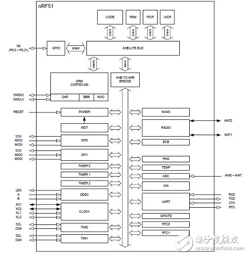
Figure 1 nRF51822 block diagram
The smart bracelet is a wearable smart device. Through this bracelet, users can record real-time data such as exercise, sleep, and some diet in daily life, and synchronize these data with mobile phones, tablets, and iPod touches to guide healthy living through data.
The smart bracelet has a built-in low-power Bluetooth 4.0 module that can be connected to mobile phones, tablets, and PC clients. It can set height, weight, stride and other information and upload motion data anytime, anywhere. In addition, the smart bracelet also has a social network sharing function, for example, the user can share the sleep quality, the eating situation and the exercise situation, and the mood record through the social network end such as binding Weibo.
The nRF51822 is a multi-protocol, single-chip solution designed for ultra-low power wireless applications. The chip supports BLE4.0 and 2.4GHZ protocol stacks, integrates RF transmit circuitry, an ARM Cortex M0 core and 256KB of flash + 16KB of RAM.
The hardware circuit design part of the bracelet includes an MCU (nrf51822) with integrated BLE function, and various peripherals controlled by the MCU:
Bluetooth radio frequency circuit;
G-sensor using SPI interface;
a linear motor drive circuit using an I2C interface;
LED dot matrix drive using I2C interface, sharing bus with linear motor;
Use GPIO's button input;
Use GPIO LED lights;
Use a normal motor drive circuit of GPIO;
External reset circuit.
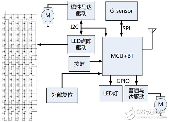
Figure 2 Smart bracelet block diagram
Smart Bracelet Main Parts Description: Smart Bracelet
1. MCU
The nRF51822 is a multi-protocol, single-chip solution designed for ultra-low power wireless applications. The chip supports BLE4.0 and 2.4GHZ protocol stacks, integrates RF transmit circuitry, an ARM Cortex M0 core and 256KB of flash + 16KB of RAM.
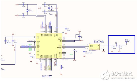
Figure 3 Smart Bracelet MCU Circuit
2. G-sensor
G-sensor is the meaning of gravity sensor (English name is Gravity-sensor), it can sense the change of acceleration force, the force that acts on the object during acceleration, such as shaking, falling, rising, falling Various kinds of movement changes can be converted into electrical signals by G-sensor, and then through the calculation and analysis of the microprocessor, the programmed functions can be completed. For example, the MP3 can change the songs before and after the user according to the direction of the user's movement. When you put it in your pocket, you can also calculate the user's progress.
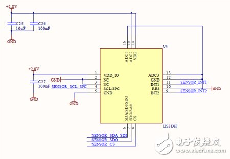
Figure 4 G-sensor circuit
3. Key input module
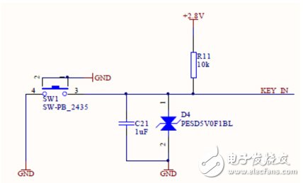
Figure 5 button input module circuit
4. LED display
LED display is a module for data interaction between the bracelet and the user, mainly used for data display and user interaction.
According to the different needs of manufacturers, two design solutions are provided:
1. LED light control display: simple information presentation in combination of multiple LED indicators.
2, LED dot array display: Display the data information of the bracelet in the form of LED dot array: time, number of steps, calorie consumption, etc.
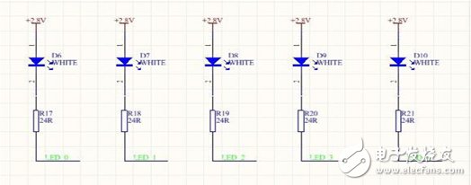
Figure 6 LED light control circuit
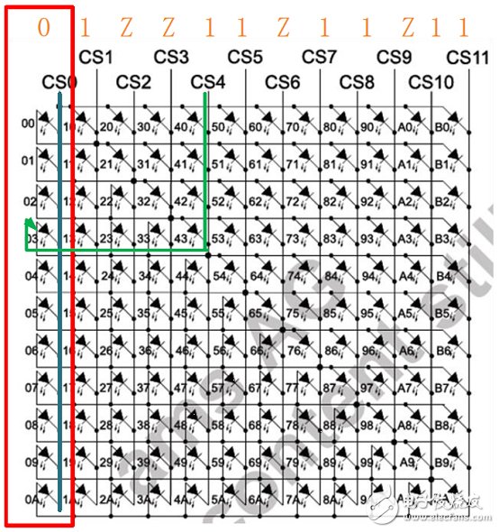
Figure 7 LED dot array control module circuit
5. Ordinary motor module
Since the on-current of the motor may be as high as 100 mA and cannot be directly controlled by the GPIO (the drive current is insufficient), a MOS transistor is used as the power amplifier circuit. A series of 24 ohm resistors are used to adjust the motor's vibration strength and reduce power consumption. At 0 ohms, the motor's starting current is about 100 mA, and the current measured current is 36 mA.
The pull-down resistor at the input of the MOS transistor ensures that the motor remains stationary at the time of restart, because the pin is high after the chip is powered up, and the MOS is in a conducting state, thus causing a brief vibration of the motor.
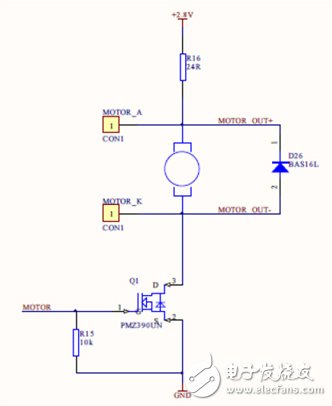
Figure 8 Ordinary motor module control circuit
6. Linear motor control module
Linear motor control is complex and requires a dedicated chip (the DRV2605 driver chip is used in the design). The chip communicates with the MCU via the I2C bus. The function of the linear motor is controlled by the driver chip, and the input voltage range of the driver chip itself is 2.5V-5.5V.
The supply voltage to the driver chip is designed to be battery powered rather than the system voltage of the DCDC output.
The reason is: the operating voltage of the driver chip is to use the internal DCDC to complete the voltage conversion. Assuming a DCDC conversion efficiency of 90%, battery power is used, energy efficiency is 90%; using system voltage supply, efficiency is 90% * 90% = 81%.
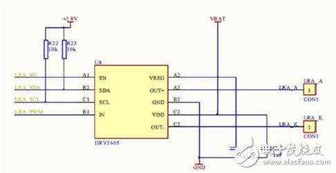
Figure 9 linear motor control circuit
7. Power detection module
The battery's power and voltage have a corresponding relationship. As long as the battery voltage is detected, the system can be mapped into the remaining battery power.
The battery voltage varies between 0 and 4.2V. After a quarter of the voltage divider circuit, the output voltage will vary from 0 to 1.05V. Taking full advantage of the nRF51822's ADC range of 0-1.2V, parallel resistors are used to stabilize the voltage.
The circuit is as follows:
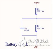
Figure 10 battery detection module circuit
8. External reset module
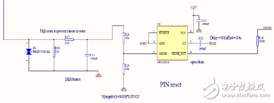
Figure 11 external reset module circuit
9. Charging circuit module
The charging chip uses TI's BQ24040. The purpose of this model is to provide the MCU with information on whether it is charging (CHG_STATE) and whether to insert the charger (PG_STATE) (most charging ICs do not provide the latter information). The charging current is controllable, and the ratio of pre-charging and fast current is controllable.
The current reference scheme is based on a 18 mAh battery with a precharge current of 40% of the fast charge current.
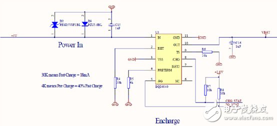
Figure 12 charging circuit module circuit
10. System power module
In order to ensure sufficient power efficiency, the design uses a high efficiency, light-load optimized DCDC chip TPS62260 instead of the traditional LDO. Because the nRF51822 has an LDO inside, in order to improve efficiency, the system voltage should be as low as possible, while the normal operating voltage of the motor is 3V, the minimum operating voltage of the white LED is 2.8V, and the minimum system voltage of other ICs is 1.8V. Therefore the final determined system voltage is 2.8V.
Power chip selection:
l The static power consumption of traditional LDOs has advantages, but the larger the input-output voltage difference, the lower the efficiency. If the battery voltage is 3.9V, the output voltage is 2.8V, and the efficiency is 2.8/3.9=71%;
l DCDC quiescent current is large, but when the input current is above 1mA, the efficiency can reach more than 90%;
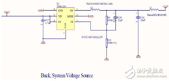
Figure 13 system power module circuit
11. Debug interface
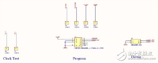
Figure 14 debug interface circuit
12. Radio frequency circuit
Keep the devices as close as possible, and shorten the traces (1mm trace is equivalent to 1nH inductor; longer line will increase capacitance to ground)
Do not use vias (vias are equivalent to inductors)
The matching circuit is wrapped by GND to reduce the capacitance to ground
Do not route or place devices under the matching network, resulting in a "black hole" between the matching network and the reference ground.
It is recommended that the board thickness not exceed 1.6mm, otherwise the RF performance will decrease.
High power and noise source signal traces should be perpendicular to the RF line
LED is a high-power signal compared to RF. If it is not a design requirement, it is strongly recommended not to place the LED near the antenna like this PCB solution (although the LED trace in the PCB has been as perpendicular to the antenna as possible)
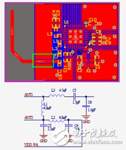
Figure 15 PCB correct routing and equivalent circuit
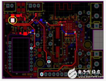
Figure 16 Smart Bracelet PCB Outline Drawing
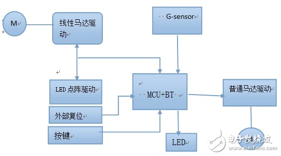
Figure 4 smart bracelet structure diagram
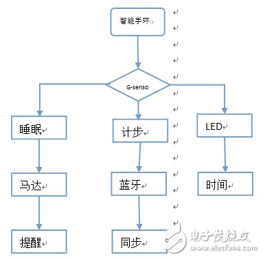
Smart bracelet function implementation flow chart
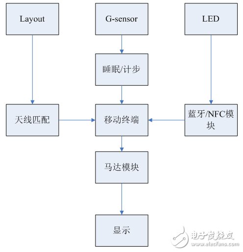
Figure 8 main program structure flow chart
1L Air Fryer,Air Deep Fryers,Power Air Fryer,Stainless Steel Air Fryer
Ningbo Anbo United Electric Appliance Co.,ltd , https://www.airfryerfactory.com