 IBM and Micron announced today that they will use the TSV (silicon perforation) process technology pioneered by Big Blue in the world to manufacture hybrid memory cube (HMC) memory chips developed by Micron, claiming to be faster than existing memory chips. Up to 15 times faster.
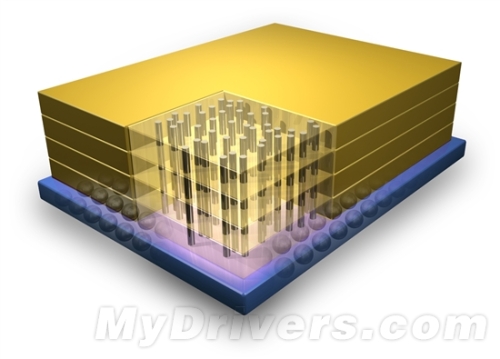
 The HMC chip uses vertical pipes (or perforations) to package multiple independent chip stacks together. The product prototype has a bandwidth of up to 128 GB/s, and the final product will be even higher, but the current average memory is still only 12.8 GB/s. At the same time, HMC can reduce the package size of the chip by up to 90%, while reducing the energy consumed to transmit data by 70%.
IBM's newly developed 3-D TSV manufacturing process is just to connect the 3D microarchitecture, and will become the basis for commercial production of HMC memory.
IBM will use the 32nm HKMG process to manufacture Micron's HMC memory chips at its East Fishkill plant in New York State. More details on its TSV technology will be announced at the IEEE International Electronic Equipment Conference recently.
The initial stage of HMC memory is for professional networks such as large-scale networks, high-performance computing, and industrial automation. However, it will eventually strive to enter consumer-grade products.
Ceramic element(External drive)
SWT Smart Technology Co., Ltd. , http://www.fuding-sound.com