>>> 4.4.1 Interrupt and event driven
Regardless of the bus type used, the clock signal and data/control lines are always present. The MCU master controls the clock signal. The SPI signal line for control consists of four signals, including the chip select signal, which allows the host to determine which device is the target by the validity of the signal.
> > > 4.6.1 Introduction to SPI Bus
This section introduces the principle and application design of the SPI bus using the LPC824 as an example.
SSEL: Chip Select Input
When the SPI is in master mode, the SSEL signal is activated before the serial data transmission starts and deactivated after it ends. By default, SSEL is active low, but it can also be configured as active high. In slave mode, an active SSEL signal indicates that the slave is being addressed.
MOSI: Master Output Slave Input
The MOSI signal transmits serial data from the master to the slave. When the SPI is a master, data is output through MOSI; when it's a slave, data is input through MOSI.
MISO: Master Input Slave Output
The MISO signal transmits serial data from the slave to the master. When the SPI is a master, data is input through MISO; when it's a slave, data is output through MISO.
SCK: Clock Signal
SCK is the synchronous clock signal for data transfer. It is driven by the master and can be programmed to be either active high or active low.
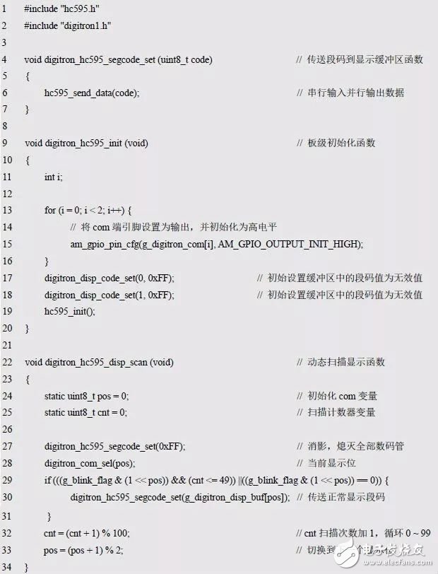
> > > 4.6.2 74HC595 Interface
The 74HC595 performs serial-to-parallel conversion under the same clock signal. It has 8 parallel outputs and 5 input control pins, including Q0-Q7, VCC, CP, D, and STR. These are connected to the MCU’s SCK, MOSI, and SSEL, respectively, as shown in Figure 4.18.
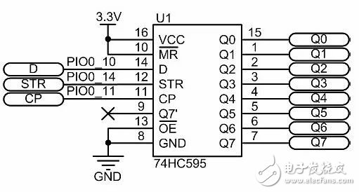
Figure 4.18 74HC595 circuit diagram
On the rising edge of the CP clock signal, the binary data on the D side is sent to the 74HC595. After shifting, the STR signal causes the data to be output at Q0-Q7, ensuring stability during the shift process.
The MiniPort-595 module uses the 74HC595 to expand 8-channel I/O, directly driving LED modules. The M4 function definition for the AMPort-Core MiniPort interface is shown in Figure 4.19(b). The J2 pin definitions for the MiniPort-595 module are given in Figure 4.19(c).
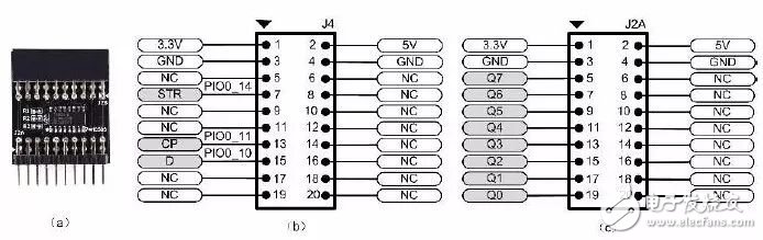
Figure 4.19 595 Module Physical and Control Interface Definition
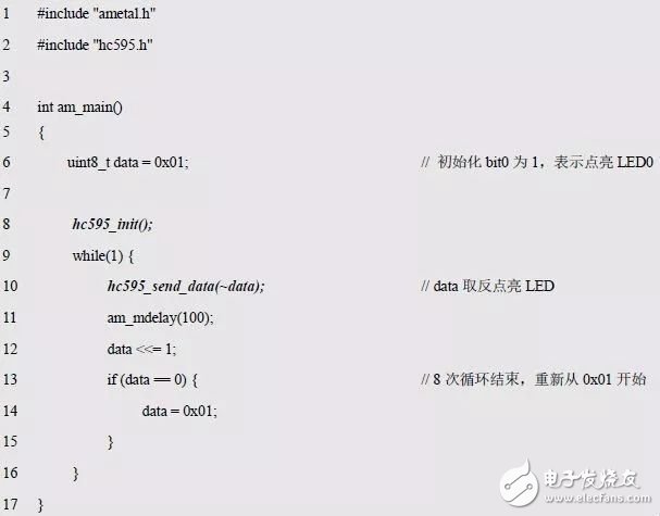
To send 1000 0000 to the 74HC595’s Q0-Q7, the data is sent bit by bit via the D terminal under the CP clock. After 8 clock pulses, the data appears in parallel at Q0-Q7. AMetal provides the hc595.h interface, as detailed in Listing 4.44.
Listing 4.44 hc595.h interface
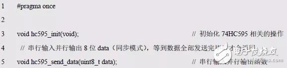
Calling hc595_send_data() after initialization allows the 74HC595 to output an 8-bit binary number in parallel, acting as an 8-bit I/O port. Previously, 8 LEDs required 8 I/Os, but now more ports are available for other functions.
The AM824-Core host, MiniPort A of the MiniPort-595 module, and MiniPort B of the MiniPort-LED module can be directly inserted, as shown in Figure 4.20. The MCU controls the 74HC595 to drive 8 LEDs through STR, CP, and D, as seen in Listing 4.45.
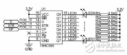
Figure 4.20 8-Output I/O Expansion
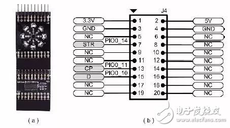
Figure 4.21 Module combination physical and control interface definition
Listing 4.45 74HC595 Universal Interface Sample Program
The 74HC595 can also drive a 2-digit digital tube, as shown in Figure 4.22.
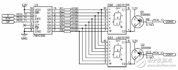
Figure 4.22 2-digit digital tube driver circuit
The MiniPort A (pin header) of the AM824-Core and MiniPort-595 modules and the MiniPort B (mother socket) of the MiniPort-View module can be directly inserted. See Figure 4.23(a). The MCU controls the 74HC595 and uses COM0 and COM1 to manage the digitron position.
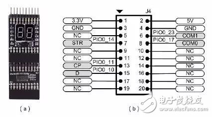
Figure 4.23 Module Combination Physical and Control Interface Definition
The only difference between using the 74HC595 and direct I/O is the segment code output method. Modify the segment code transfer function and add the implementation code to digitron1.c, as shown in Listing 4.46.
Listing 4.46 adds the relevant function of the 74HC595 driver
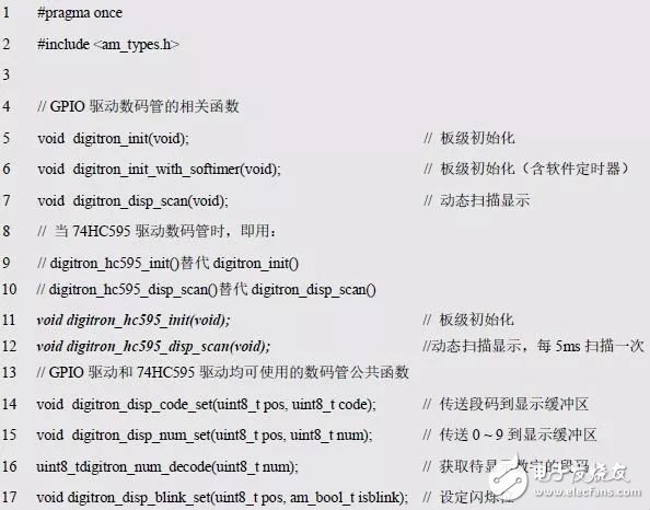
Only digitron_hc595_init() and digitron_hc595_disp_scan() are called in the digitron1.h interface, as shown in Listing 4.47.
Listing 4.47 digitron1.h
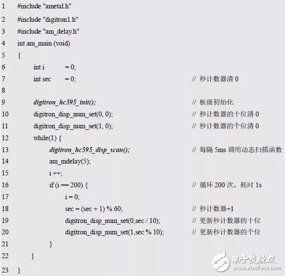
When using the 74HC595 to drive a digital tube, simply call the relevant functions, as shown in Listing 4.48.
Listing 4.48 74HC595 driver digital tube implementation seconds counter sample program
4.7 I 2 C bus
> > > 4.7.1 Introduction to I 2 C Bus
The I2C bus (Inter Integrated Circuit) is a two-wire bus developed by NXP to connect microcontrollers and peripheral devices. It offers simple hardware circuits, reusability, and portability. It is suitable for communication between devices on the same board and even between boards using a repeater, making it easy to build system-level electronic products with I2C devices. Key features include:
- Only two signal lines are needed, reducing board space and chip pin count, thus lowering interconnection costs.
- Multiple devices can be mounted on the same I2C bus, distinguished by different addresses, eliminating the need for additional I/O or address decoders.
- Easy to implement self-test functions to detect bus abnormalities quickly.
- Electrically compatible, with open-drain I/O allowing 3V/5V logic level compatibility via pull-up resistors.
- Supports multiple communication methods, including one master, dual-host, multi-master, and broadcast modes.
- High communication speed: 100Kbps (standard), 400Kbps (fast mode), and up to 3.4Mbps in later versions.
> > > 4.7.2 LM75B Interface
The AM824-Core selects the LM75B digital temperature sensor, which is compatible with LM75A and consumes only 1μA in shutdown mode.
1. Characteristics
The LM75B is a digital temperature sensor with an I2C interface from NXP Semiconductors. Its key features include:
- Device address: 1001xxx, supporting up to 8 devices on the same bus.
- Power supply range: 2.8 ~ 5.5V, temperature range: -55 ~ 125°C.
- 11-bit ADC with 0.125°C resolution.
- Accuracy: ±2°C (-25 ~ 100°C), ±3°C (-55 ~ 125°C).
The pin layout of the LM75B is shown in Figure 4.24. The slave address is 0x90. A0~A2 are address selection bits, and pull-up resistors must be added to SCL and SDA. When overheated, the output turns off.
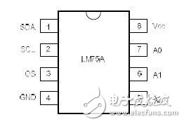
Figure 4.24 LM75B pin diagram
2. Application Circuit
The typical application circuit for the LM75B is shown in Figure 4.25. R5 and R6 are pull-up resistors for the I2C bus. Since there is only one LM75B on the board, A0~A2 can be grounded. The OS is the overheating output, which can be controlled externally via a relay. Since the temperature is measured by the MCU, this pin can be left floating. By shorting (J13_1, J13_2) and (J11_1, J11_2), SDA and SCL are connected to PIO0_18 and PIO0_16, respectively.

Figure 4.25 LM75B Application Circuit Diagram
Figure 4.26 shows the heating circuit of the AM824-Core. R32 has a resistance of 20~50Ω (2W). Shorting J14_2 and J14_3 connects the heating resistor R32 to the KEY. When the KEY button is pressed, R32 heats up, transferring heat to the bottom of the LM75B through thicker wires. The LM75B then follows the temperature rise. The lower the resistance, the higher the current and the more heat generated. Pressing the button turns on the circuit, and the temperature can be observed through the measuring circuit.
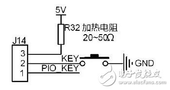
Figure 4.26 Heating circuit
3. Temperature Measurement
AMetal provides a software package for the LM75B, with the function prototype as shown. Using these interfaces, reading the current temperature value is straightforward. Since there are only two digital tubes, only the integer part is displayed. If the temperature is negative, it will not show a negative sign, just the numeric value. Details are provided in Listing 4.49.
Listing 4.49 LM75 Temperature Reading and Display Sample Program
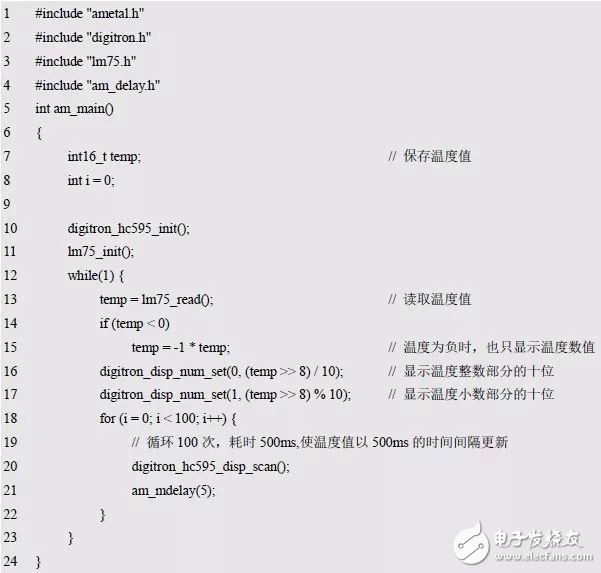
After compiling and downloading the program to the development board, if the digital tube displays 28, the current temperature is 28°C. Pressing the heating button activates R32, causing the displayed temperature to increase.
When displaying the temperature value, the value is shifted right by 8 bits because lm75_read() returns a value 256 times the actual temperature. Shifting right by 8 bits divides by 256, leaving only the integer part.
> > > 4.7.3 Thermostat
This section combines previous programs to use LED, buzzer, digital tube, matrix keyboard, and temperature acquisition to create a simple thermostat.
1. Function Introduction
The temperature is collected using the standard I2C interface LM75B sensor and displayed on the digital tube. Only the integer part is shown due to the limited number of digital tubes. Negative temperatures do not display a minus sign.
The upper and lower temperature limits can be set. If the temperature exceeds the upper limit or falls below the lower limit, the buzzer will sound.
2. Status Indication
Two LEDs indicate status during adjustment, with J9 and J10 connected via a short-circuit jumper.
- LED0 on: Indicates the current value is the upper limit, and the digital tube displays the upper limit.
- LED1 on: Indicates the current value is the lower limit, and the digital tube displays the lower limit.
- Both lights flashing: Indicates normal operation, and the digital tube displays the ambient temperature.
3. Instructions
Four buttons are used to set the upper and lower limits:
- SET button: Enters the setting state. Click once to enter the upper limit setting, again to enter the lower limit setting, and again to return to normal operation.
- Left/Right Shift key: Switches the currently adjusted bit (one digit/ten digit). When in setting mode, the current bit flashes continuously. Pressing this key switches between digits.
- Add 1 key: Increases the value of the current flashing bit.
- Subtract 1 key: Decreases the value of the current flashing bit.
(1) Set the Upper Limit
Press the SET button to enter the upper limit setting. LED0 lights up, the digital tube displays the upper limit, and the single digit stops flashing. Use “Add 1†or “Subtract 1†to adjust the current flashing bit. Press “Left/Right†to switch the current bit.
(2) Set the Lower Limit
After setting the upper limit, press the SET button again to enter the lower limit setting. LED1 lights up, the digital tube displays the lower limit, and the single digit blinks. Adjust the current flashing bit using “Add 1†or “Subtract 1â€, and use “Left/Right†to switch the current bit.
4. Function Realization
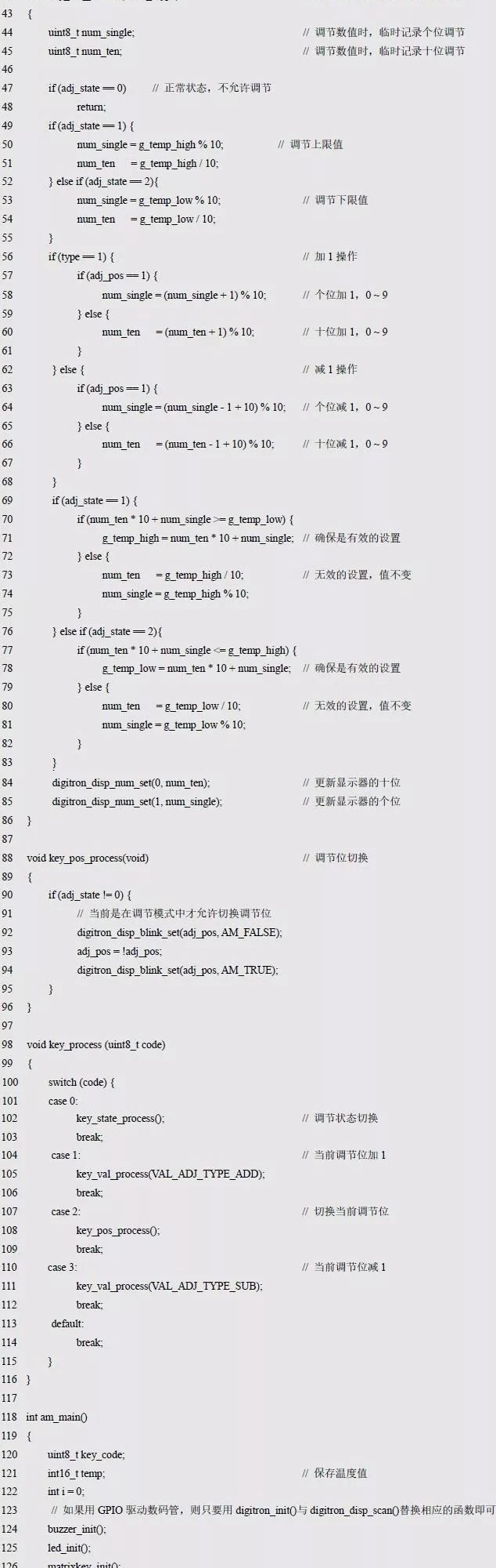
As shown in Listing 4.50, the thermostat sample program is more complex. To improve clarity, three functions are written for each of the three buttons: switching states (KEY0), switching the current adjustment bit (KEY2), and adjusting the current bit value (KEY1 and KEY3). These functions are called in key_process(). Other parts are handled in the main loop, completing three tasks every 500ms, 10ms, and 5ms, respectively: temperature acquisition, keyboard scanning, and digital tube scanning.
Listing 4.50 Comprehensive Experimental Sample Program
Hydraulic DC motor is a device that converts electrical energy into hydraulic energy. The power transmission through the hydraulic system has the characteristics of high efficiency and stability. Therefore, they are often used in applications requiring high torque and low speed movement, such as industrial equipment, the automotive industry, agricultural machinery and ships. The power transmission through the hydraulic system has the characteristics of high efficiency and stability.
Hydraulic Dc Motors,Hydraulic Dc Motor,Dc Hydraulic Pump,Dc Hydraulic Pump Motor
Wuxi Jinle Automobile Motor Factory , https://www.wxjldj.com