First, transparent substrate technology
The InGaAlP LED is usually prepared by epitaxially growing a GaP window region of an InGaAlP light-emitting region on a GaAs substrate. Compared with InGaAlP, GaAs materials have much smaller band gaps. Therefore, when short-wavelength light is incident on the GaAs substrate from the light-emitting region and the window surface, it will be absorbed in full, which is the main reason for the low light-emitting efficiency of the device. . A Bragg reflection region is grown between the substrate and the confinement layer, and the light that is directed perpendicularly to the substrate can be reflected back to the illuminating region or window, partially improving the light-emitting characteristics of the device. A more efficient method is to first remove the GaAs substrate and replace it with a fully transparent GaP crystal. The quantum efficiency is increased from 4% to 25-30% due to the removal of the substrate absorption region within the chip. In order to further reduce the absorption of the electrode region, the transparent substrate type InGaAlP device is formed into a truncated inverted cone shape, which further improves the quantum efficiency.
Second, metal film reflection technology
The transparent substrate process first originated from companies such as HP and Lumileds in the United States. The metal film reflection method mainly has a lot of research and development by Japanese and Taiwanese manufacturers. This process not only avoids the transparent substrate patent, but also is more conducive to mass production. The effect can be said to be similar to the transparent substrate method. This process is usually referred to as the MB process. First, the GaAs substrate is removed, and then an Al metal film is vapor-deposited on the surface thereof simultaneously with the surface of the Si substrate, and then welded together under a certain temperature and pressure. Thus, the light irradiated from the light-emitting layer to the substrate is reflected by the Al-metal film layer to the surface of the chip, thereby improving the luminous efficiency of the device by 2.5 times or more.
Third, surface microstructure technology
Surface microstructure process is another effective technology to improve the light extraction efficiency of the device. The basic point of this technology is to etch a large number of small structures on the surface of the chip with the size of light wavelength. Each structure has a truncated tetrahedron shape, which not only expands. The light-emitting area is changed, and the direction of refraction of light at the surface of the chip is changed, so that the light-transmitting efficiency is remarkably improved. Measurements indicate that for devices with a window layer thickness of 20 μm, the light extraction efficiency can be increased by 30%. When the window layer thickness is reduced to 10 μm, the light extraction efficiency will be improved by 60%. For the 585-625nm wavelength LED device, after the texture structure is fabricated, the luminous efficiency can reach 30lm/w, and the value is close to the level of the transparent substrate device.
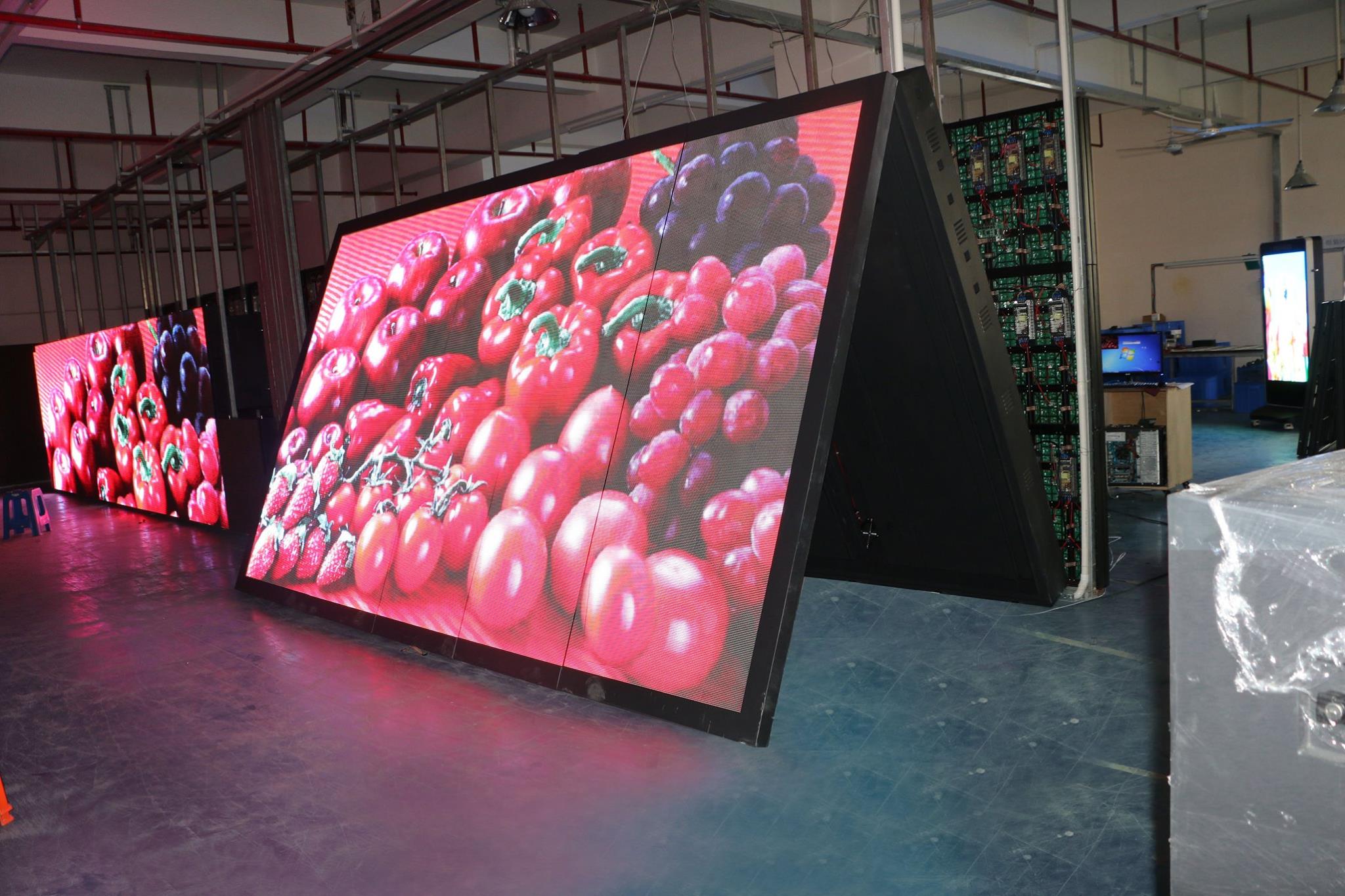
The biggest features of Front Service Led Display is is to save space! For the indoor or mosaic installation structure, the empty space is very small that not convenient for the maintenance. The outdoor front service Led Display is mainly use for front open cabinet, which can greatly reduce the overall thickness of the led display structure, and can not only be well integrated with the surroundings, but also can save the space while ensure the effect.

Front Service Led Display
Front Service Led Display,Led Wall Panel,Led Scrolling Text Display,Led Indoor Display
Shenzhen Cxcolor Optoelectronics Co., LTD. , http://www.largeledscreen.com