Professor Zhou Ligong’s new book, "Programming for AMetal Frameworks and Interfaces (Part 1)", offers a comprehensive introduction to the AMetal framework. By studying this book, readers can gain insights into advanced software design principles and development approaches for interface programming. It encourages focusing on your core domain, evolving your programming mindset, and achieving mutual growth between the company and the individual. Authorized by Professor Zhou Ligong, the Zhiyuan Electronic Public Number will serialize the content of the book, sharing it with the community.
The second chapter focuses on ADC signal conditioning circuit design, covering sections 2.3 Necessary Measures, 2.4 Actual Test Verification, and 2.5 Application Description.
2.3 Necessary Measures
A typical acquisition circuit block diagram is shown in Figure 2.19. From the sensor or signal source to the final ADC output, signal conditioning such as input range adjustment and multi-channel multiplexing is essential. In addition to the ADC itself, the entire acquisition channel must be carefully designed to ensure high accuracy.

Figure 2.19 Typical Acquisition Circuit Block Diagram
Key considerations when designing the acquisition channel include:
- The size of the signal and the ADC's full-scale input range.
- The polarity of the signal and the ADC input.
- The number of channels and whether simultaneous sampling or multiplexed input is needed.
- Whether the signal is single-ended or differential.
2.3.1 Input Range Matching
Sensor signals are often weak, and their amplitude may only occupy a small portion of the ADC range. Matching the maximum input signal to the ADC range is crucial for maximizing conversion accuracy. For example, if the signal ranges from 0V to 2V, and VREF is 3V, the ADC value at 2V would be 2729, leaving 1366 unused values, which reduces overall accuracy.
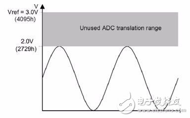
Figure 2.20 Input Signal Amplitude and ADC Measurement Range
To improve this, an external preamplifier can be used to scale the input signal to match the ADC range. For instance, using LMV358A as a 10x non-inverting amplifier can convert a 0–300mV input to 0–3V. Alternatively, an external amplifier can be used to handle bipolar inputs, converting them to unipolar, or an instrumentation amplifier can convert differential inputs to single-ended.
2.3.2 Multi-channel Sampling Setup
When cost is a concern, multiple channels can share one ADC. The LPC82x has 12 analog input pins, but the internal structure allows for time-division multiplexing. However, this setup can introduce issues like excessive signal source impedance and crosstalk due to parasitic capacitance.

Figure 2.21 Multiplexed Equivalent Circuit of LPC82x Analog Input Channel
To mitigate these problems, a hybrid configuration is often used: adding an op amp to high-accuracy channels while directly connecting low-accuracy ones. This approach requires careful consideration of signal speed and bandwidth.

Figure 2.22 Multi-channel Sampling Circuit for High-speed Signals
The maximum allowable source impedance depends on the sampling rate. For example, with a 12-bit ADC at 1 Msps, the setup time must be sufficient to ensure accurate sampling. If the source impedance is too high, the sampling time must be increased to maintain accuracy.
2.3.3 Power Distribution Strategy
Power supply noise can significantly affect performance. To reduce interference, it is recommended to power the analog and digital sections separately using voltage regulators.
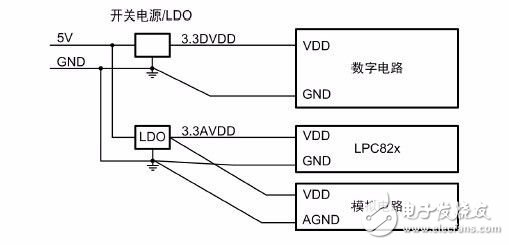
Figure 2.25 Analog and Digital Parts Powered Separately
2.3.4 PCB Layout Processing
Digital switching noise can interfere with analog circuits. To prevent this, place analog and digital components in separate sub-regions, split the ground plane, and avoid parallel traces. Ground traces can also be added between analog and digital traces to reduce interference.

Figure 2.27 Split Ground Plane with Single Point Connection
2.4 Measured Verification
A test board was built to verify the effectiveness of the improvements. Key parameters like noise-free resolution, INL, offset error, and gain error were tested and compared with the original AM824 development board.
2.4.1 Noise-free Resolution
Noise-free resolution refers to the number of stable bits in the ADC output when measuring a DC signal. On the original AM824 board, the resolution was limited to 9 bits, but after improvements, it reached 10 bits, showing better accuracy.
2.4.2 Integral Nonlinearity (INL)
INL measures the deviation of the actual ADC output from an ideal line. After improvements, the INL improved from 5.3 LSB to 3.6 LSB, showing better linearity.
2.4.3 Offset and Gain Error
Offset error is the deviation at the first transition, while gain error is the deviation at the last transition. Both were measured and showed significant improvement after the design changes.
2.5 Application Notes
Summary of test results shows that the improved design achieves higher accuracy, suitable for applications requiring 0.5% precision. Users can adjust parameters like filter bandwidth or input range with minimal changes to the circuit.
4.2Mm Ribbon Connector,Strip Connectors,Strip Terminal,Strip Connector
YUEQING WEIMAI ELECTRONICS CO.,LTD , https://www.wmconnector.com