The AIS system is a collision avoidance system that uses TDMA technology to exchange data in the maritime mobile VHF band. It is one of the equipment that must be installed on each vessel as required by the International Maritime Organization. The product development is based on the ITU-R M1371 protocol promulgated by the International Maritime Organization. In the development, using ADSP2189M as its data processing platform, it completes various data processing, conversion, time slot division, network login and maintenance algorithms, and realizes most of its main functions. The pattern of the system is shown in Figure 1.
The radio station receives the GMSK signal at the two frequency points of 161.975MHz and 162.025MHz, and converts the analog data into a digital signal through the GMSK modulation and demodulation chip. The data stream passes the upper computer to complete the judgment of the correct data, and deletes the data segment. Start, fill and end bits, send the data to the DSP through the parallel port, the DSP completes the processing and analysis of the received data, establishes the time slot table of the entire sea area, completes the TDMA network login and maintenance, and transfers the relevant data to the Different formats are sent to different serial ports for output. According to the ITU-R M.1371 protocol, it is connected to the network in ITDMA (Incremental Time Division Multiple Access) mode, and it runs continuously in SOTDMA (Self-Controlled Time Division Multiple Access) mode to achieve TDMA of the entire network. Completeness. Therefore, the signal processing unit is in an important position in the system.
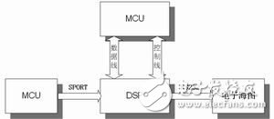
Figure 1 DSP and external equipment interface
ADSP2189M chipThe ADSP2189M chip is a fixed-point DSP with an instruction cycle of 13.3ns and a running speed of up to 75MIPS. The processor includes arithmetic/logic unit (ALU), multiplier/accumulator (MAC) and barrel shifter. The memory adopts Harvard structure, with 48K PRAM and 32K DRAM. Two SPORT synchronous serial ports, a timer and host interface can be directly connected to the host processor. DMA interface includes internal DMA interface (IDMA) and byte DMA interface (BDMA).
The hardware design of 2189M in AIS systemPart of the circuit is shown in Figure 2.
·The chip is connected to a 33M crystal, and its internal frequency is automatically multiplied to 66M;
·A synchronous serial port SPORT is connected to an external MCU, and the pin must be connected to a pull-up resistor;
·Set SPORT1 to the second working mode, and use the software to simulate the UART of the I/O port, connect it with the MAX232 chip, and send the data to the simple display;
·Using the IDMA method to connect with the MCU, 16 parallel port lines, the startup mode is set to IDMA, and the 4 MODEA~D settings are 1, 0, 1, 0 respectively;
·The steps to complete IDMA boot loading are as follows;
The four debugging pins of PWD, EBR, BR, and ERSET must be connected with pull-up resistors;
Finally, write the value of PM (0X0000), and the program will start to execute automatically.
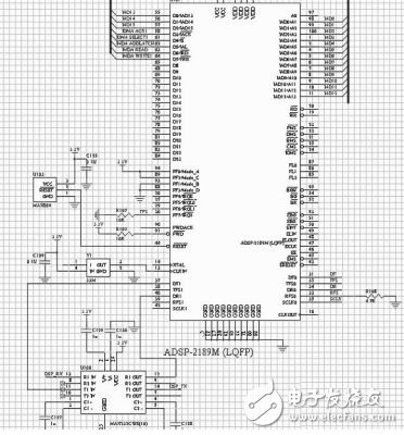
Figure 2 Part of the circuit diagram of the AIS system
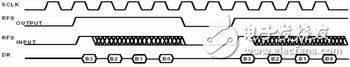
Figure 3 Sequence diagram of serial port reception
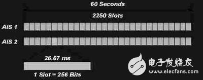
Figure 4 Time slot division diagram
The software design of ADSP2189M interface
Sport0 settingsUse synchronous serial port to communicate with MCU
DM (0X3FF6)—The serial port control register settings are shown in Table 1.
In Table 1, 0~3: receive and send word length, we define it as 16-bit word length, set to 1111. 6~7: frame synchronization signal level, it is 0, high level is effective. 8~9: Frame synchronization signal source, set to 1, internally generate frame synchronization signal.
10~11: framing mode, 1, the second framing mode. 12~13: Frame synchronization, 0, frame synchronization signal is required to initiate communication, and frame synchronization signal will not be considered in the future. 14: The generation mode of SCLK is 1, the serial clock is generated internally.
DM (0X3FF5)-serial port clock frequency division coefficient register dm (sclkdiv)
In the ADSP2189 chip, the relationship between the sampling rate and the frequency division number is as follows: F(sclk)=f(clkout)/(sclkdiv+1)/2
Among them, F (sclk) represents the operating clock, F (clkout) represents the output clock of the external crystal oscillator, and sclkdiv represents the frequency division number, that is, the value that the memory should assign.
When the control register is set, the serial port receiving sequence is shown in Figure 3. The received data is placed in the receiving buffer area. After receiving a group of data, the receiving flag bit is written once. The main program periodically checks the flag bit. When the flag is detected When the bit changes, call the receive processing subroutine.
Sport1 and timer settingsBecause the DSP wants to output data to the simple display, which is connected through the UART port, set Sport1 to the second working mode (as shown in Table 2).
DM (0X3FFF)-System control register (as shown in Table 3).
In Table 3, 12: SPORT0 enable, set to 1. 11: SPORT1 enable, set to 1. 10: SPOER1 function selection, set to 0.
I/O port is used to simulate UART, sampling at 9600 baud rate, internal timing interrupt generation rate is 3×9600, 3 samples are generated in a level transition, and the middle sampling value is valid.
DM (0X3FFD)-timing period register
DM (0X3FFC)-timer counting register
Connect 33M crystal, the value stored in the register is:
period=frequence×2/(3×9600)-1=2314
The chip generates an interrupt at a baud rate of 28800. Each time the interrupt program detects the flag bit of the UART, when the flag bit changes, the I/O output is set once every three interrupts until the end of the sending data.
Some code settings are as follows:
ax0 = 2314; //Timer setting
dm(0x3ffc) = ax0;
dm(0x3ffd) = ax0;
ax0 = 0;
dm (0x3ffb) = ax0; //Settings of control registers
ax0 = b#0001100000000000;
ax0=b#0111111000001111;
dm(0x3ff6)=ax0; //sport0 setting
ax0=0x001f;
dm(0x3ff5)=ax0; //SCLKDIV0
mstat = 0x10; // Multiplier settings
ifc=b#0000000001100001; imask=b#0000100001; //open interrupt
ena TImer;
//Turn on timing
Main software processThe system adopts autonomous time division multiplexing, dividing time into periodic frames, and each frame is divided into several time slots (no matter the frame or time slot is mutually non-overlapping), each time slot is a communication channel, which is allocated to One user. The system is based on a certain time slot allocation principle, so that each mobile station can only transmit signals (burst signals) to each other according to the designated time slot in each frame. Under the condition of meeting timing and synchronization, the base station can be in each time slot Receive signals from each mobile station without interfering with each other.
The space of the two channels is divided in the register as the time slot table of the sea area, as shown in Figure 4.
The network login uses the probability persistence algorithm (when a candidate time period is found, the station randomly selects a probability value LME.RTP1 between 0 and 100, which is compared with a probability LME.RTP2 from 0 to 10, if LME.RTP1 If it is less than or equal to LME.RTP2, this time period is selected, otherwise, LME.RTP2 plus a probability increment is compared with the next candidate time period). Randomly select a free time slot as the access point of the network in 2250 time periods, and then access it in ITDMA mode. This method is a form of reporting first, indicating the next time slot number that needs to be sent in the currently transmitted data, so as to notify other stations in advance of the number of the time slot occupied by themselves, which is determined in 60 seconds. Need to take up space. In the subsequent successive stages, the mobile station completes the maintenance of the network and the re-division of time slots in SOTDMA mode. Since the data format specified in the protocol can only predict the occupancy for up to 7 minutes, it is necessary to select a new free time slot within a certain range for transmission every 7 minutes, and so on, always in this continuous state Keep running.
When the speed changes, the system re-completes the network login under the new speed in the way of ITDMA.
ConclusionThe design proposed in this paper makes full use of the high-performance data processing functions of DSP and the real-time and stable characteristics of embedded operating systems, and uses time-division multiplexing algorithms to perform network division and connection functions in a sea area. This mode of combining DSP signal processing and embedded operating system can be widely used in the communication field and has a wide range of application prospects.
Elf Bar,Elf Bar With All The Flavors,Raspberry Elf Bar,Elf Bar 1500 Vape
Shenzhen Zpal Technology Co.,Ltd , https://www.zpalvapes.com