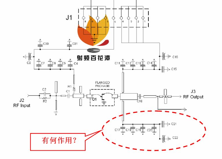
The CGH40045F-TB drain bias circuit adopts a symmetric design. The main reason for this analysis is to reduce the impedance of the bias network and increase the video bandwidth VBW, thereby reducing the electrical memory effect of the power amplifier tube.
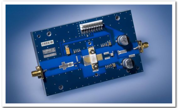
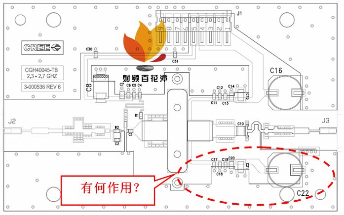
Figure 1 CGH40045-TB PCB
The following is a brief introduction to VBW and electrical memory effects:
The bandwidth of the low-impedance path is called video bandwidth (VBW) and ranges from 100 KHz to 200 MHz. The individual understands that the bandwidth of the modulation signal, ie, the channel bandwidth, is related to the input modulation signal.
The memory effect of the power tube is divided into the thermal memory effect and the electrical memory effect. The thermal memory effect is mainly related to the temperature cycle of the transistor channel. The electrical memory effect mainly comes from the DC bias of the power amplifier circuit. The essence of the memory effect is that the current moment is not only related to the input signal but also related to a certain moment in the past, which is reflected in gain and phase.
When the power amplifier tube is in the digital predistortion scheme, it is particularly important to reduce the effect of the memory effect on the power amplifier. The bias circuit is an important source of the memory effect. In reality, the circuit impedance between the drain and the power supply of the power tube ( The video impedance is not zero at low frequencies (VBW 10MHz). The presence of this impedance makes the voltage applied to the drain of the power transistor not a constant value, but changes with the input signal of the amplifier. If it is purely resistive, it will only cause gain compression, and if there is a reactive portion, it will cause a memory effect. Therefore, in the design, the impedance needs to be as small as possible. At the same time, engineering experiments show that in the same input signal and the same DPD system, the ACPR of the larger video bandwidth (VBW) is better than the ACPR of the smaller video bandwidth (VBW).

Figure 2 Transistor VBW Calculation Formula
Figure 2 shows that fr represents the low-frequency resonant frequency of the transistor output section. The higher the frequency is, the wider the VBW is. Ltot is the equivalent inductance of the supply line and the bypass capacitor. Ctot is between the transistor drain stages. Capacitance, so the measure to improve VBW in operability is to reduce Ltot.
The specific measures are as follows:
1. As shown in Figure 1, the double-supply mode of the drain stage reduces the impedance in parallel and reduces the influence of the low-frequency signal.
2. Place the uF-class capacitor close to the drain, the operating frequency of the capacitor is actually greater than its SFR, so that the capacitor is inductive, thus reducing the Ltot and increasing the VBW.
3. Shorten the length of the drain supply line, less than 1/4 wavelength, but this will sacrifice some of the power.
Android is an open source mobile operating system based on Linux platform released by Google at the end of 2007, and then improved for use in netbooks and MIDs. The platform consists of operating system, user interface and application software, and is claimed to be the first truly open and complete mobile software for mobile terminals.
To put it simply, the Android system is actually a very open system. It can not only realize the functions of the most commonly used notebook computers, but also realize various directional operations like mobile phones. Moreover, it is specially designed for mobile phones. The operating system developed for equipment has advantages in system resource consumption and human-computer interaction design. It is an operating system that combines traditional and advanced advantages.
New Android Tablet,Android Tablet,New Android Tablet
Jingjiang Gisen Technology Co.,Ltd , https://www.gisentech.com