Abstract: This applicaTIon note describes how to erase / write the program and data flash in the MAXQ7665 microcontrollers (µC) using the built-in uTIlity ROM. This informaTIon applies only to the MAXQ7665 flash-based microcontrollers (µC) with sector-erasable ( SE) flash.
IntroducTIonThis application note describes how to manage the internal data and program flash in the MAXQ7665 flash-based microcontrollers (µC) with sector-erasable (SE) flash memory. This discussion includes general information for performing in-application programming (IAP) of the program flash.
Memory MapsThis section details the general flash information and memory organization for various memory sizes of the MAXQ7665 devices. There are two types of flash memory available on the MAX7665 devices. This document only covers the MAXQ7665 devices with SE flash and does not apply to the page -erasable (PE) devices. For information on MAXQ7665 PE devices, please refer to application note, "In-Application Programming (IAP) of the MAXQ7665 Page-Erasable (PE) Program and Data Flash".
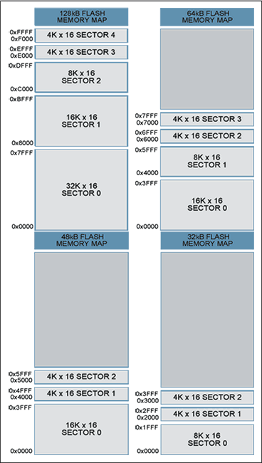
Table 1 shows the flash memory maps for the 128KB, 64KB, 48KB, and 32KB devices. Other flash options may exist, so please consult the MAXQ7665 data sheet for a complete list.
Table 1. Flash Memory Maps
Using Flash to Store Data The flash can be used to reliably store system data that needs to be programmed once or periodically during system operation. While any sector of flash can be used to store data, the two 4K x 16 sectors usually provide the best fit. Unlike EEPROM, flash on the MAXQ7665 cannot be word erased. A complete sector must be erased at one time. Erasing a sector typically takes 0.7 seconds, but can take as long as 15 seconds under worst-case conditions. During this time the user code is stalled so no other processing can occur. These limitations must be considered carefully when you choose the software technique appropriate to your system requirements. For most periodic data-storage needs, a bounded queue and / or a bank switching technique will meet the reliability requirements and needs of the system. Simple examples of both techniques follow.
Bounded QueueA bounded queue is a queue limited by a fixed number of items. This technique is commonly used whenever periodic data is processed. For example, the 4K x 16 flash sector can be divided into 64 64-word entries, which would result in the memory map in Table 2 for the 128kB part.
Upon initialization, a startup routine can scan the queue entries to determine the next available entry in the queue. Once the queue is full, it must be erased before another entry can be written. (Note: if all entries are needed, then you must also use bank switching to maintain all the data.) Once the flash is erased, the new entry can be written. The drawback to this approach is that all data can be lost if there is a drop in power during the erasing process. If the bounded-queue technique does not meet the system's requirements, then bank switching will also be needed.
Figure 1 illustrates the flow of entries into a bounded queue.
See Appendix A for a simple C source-code example.
Table 2. Example of a Bounded-Queue Memory Map
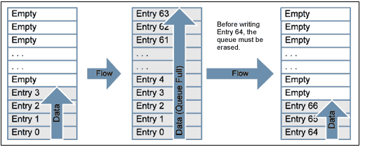
Figure 1. Bounded queue flow.
Bank SwitchingBank switching is an effective method of preventing data loss or corruption during the long sector-erase cycles. This method works well when the sector size is only slightly larger than the total data size. The drawback to bank switching is that it requires minimally two sectors of flash. When the total data size to be written is much smaller than the sector size, the best approach combines bank switching and bounded queue techniques. If bank switching is necessary for the application then, the two 4K x 16 flash sectors of the MAXQ7665 can be used as data storage.
Table 3 is an example of a memory map when using two 4K x 16 flash sectors. Figure 2 illustrates the bank-switching write / erase flow.
See Appendix A for a simple C source-code example.
Table 3. Example of a Bank-Switching Memory Map
Figure 2. Bank switching flow.
Bounded Queue and Bank SwitchingUsing the bounded-queue and bank-switching techniques together is the most reliable and flexible approach. This combined approach works well when small amounts of data need to be stored to flash periodically, and when data integrity must be maintained. Table 4 shows an example of a memory map using the two 4K x 16 sectors divided into 64 equal entries. Figure 3 illustrates the flow of data in the bounded queue between the two sectors.
The coding for this combined technique is only slightly more complex than a bounded queue alone. See Appendix A for a simple C source-code example.
Table 4. Example of a Bounded-Queue Memory Map
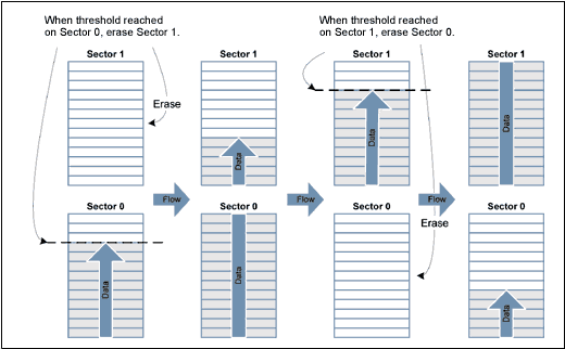
Figure 3. Flowchart for bounded queue and bank switching.
Utility ROM Flash RoutinesTo program, erase, and verify flash, the MAXQ7665 microcontroller has on-chip flash-support routines residing in ROM (read-only memory). There are two ways to access these routines. The first and fastest method is direct access , that is to directly call the routine. To do this, provide a header file with the following lines:
u16 flashEraseSector (void *); u16 flashEraseAll (void); u16 flashWrite (void * pAddress, u16 iData); Next, add linker defines to assign the appropriate address for each routine. For the IAR linker file, the added lines would look like this:
-DflashEraseSector = 0x8XXX -DflashEraseAll = 0x8XXX -DflashWrite = 0x8XXX Replace 0x8XXX with the appropriate memory address for each routine. Other compilers might use a different method for adding these references.
Note: the direct-access method does not provide forward compatibility with future ROM versions.
The second method of indirect addressing uses a table lookup. While this method provides greater compatibility with future ROM versions, it consumes greater execution time. After each routine described below, an assembly routine uses the table-lookup method to obtain the address of the ROM Utility routine. Table 5 shows the flash routines supplied by the Utility ROM. For a complete listing of ROM Utility routines, please refer to the MAXQ7665 User's Guide which can be found o the Maxim website.
Table 5. Flash Utility ROM Routines
flashWrite
The following example of assembly code calls the flashWrite () utility routine using the indirect addressing method (lookup table). This routine is callable by C code.; This routine is callable by C code using the following prototype; u16 flashWrite (void * pAddress , u16 iData);; flashWrite: move APC, # 0; No auto inc / dec of accumulator. move DP [0], # 0800Dh; This is where the address of the table is; stored. move ACC, @DP [0 ]; Get the location of the routine table. Add # 14; Add the index to the flashWrite routine. Move DP [0], ACC move ACC, @DP [0]; Retrieve the address of the routine. Call ACC; Execute the routine. ret; Status returned in A [0]. flashEraseSector
; This routine is callable by C code using the following prototype; u16 flashEraseSector (void * pAddress);; flashEraseSector: move APC, # 0; No auto inc / dec of accumulator. Move DP [0], # 0800Dh; This is where the address of the table is; stored. move ACC, @DP [0]; Get the location of the routine table. add # 1; Add the index to the flashEraseSector routine. move DP [0], ACC move ACC, @DP [0]; Retrieve the address of the routine. Call ACC; Execute the routine. Ret; Status returned in A [0] flashEraseAll
; This routine is callable by C code using the following prototype; void flashEraseAll (void);; flashEraseAll: move APC, # 0; No auto inc / dec of accumulator. Move DP [0], # 0800Dh; This is where the address of the table is; stored. move ACC, @DP [0]; Get the location of the routine table. add # 2; Add the index to the flashEraseAll routine. move DP [0], ACC move ACC, @DP [0 ]; Retrieve the address of the routine. Call ACC; Execute the routine. Ret In-Application Programming (IAP) Most flash-based systems must have the ability to update firmware while the system is installed in the end product. This procedure is known as In-Application Programming (IAP). The following discussion outlines general guidelines for creating an IAP application.
The Utility ROM flash routines outlined in the previous section perform all the actions necessary to erase and write the flash ROM. It is, therefore, possible for an end-user application to perform operations on the flash memory. Like any other subroutine call, control will return to the end-user's code after completion of the routine.
Care must be taken when executing an IAP sequence on sector-erase-only versions of the MAXQ7665 since no dedicated boot-loader flash sector exists. To design a fully fault-tolerant IAP, the boot-loader application must be separate from the main application . This ensures that the reprogramming procedure can be retried even after an incomplete reprogramming sequence has occurred. If IAP must tolerate failures such as power loss during the reprogramming sequence, then select a MAXQ7665 version with page-erase capability. This will allow the boot- loader application to start at 0x0000 (the reset entry point), and be fully separate from the main application code. For applications that do not require a fully fault-tolerant IAP, then IAP can be accomplished using a RAM-based reflash routine.
IAP Using a RAM-Based Flash RoutineA RAM-based flash routine can be used to reflash the MAXQ7665 when fault recovery is not required. This method requires that the main application copy a small relocatable flash-programming routine into RAM and then jump to the routine . When executing code from RAM, there are several restrictions that must be considered.
Table 6. Restrictions When Executing Code from RAM
Typically, the flash routine will communicate through either the UART or CAN interface. It is usually best to receive small packets of data and send an acknowledgement to allow for a more robust error-recovery mechanism. Figure 4 is a flowchart showing how a reflash routine can work. If reprogramming is not successfully completed before loss of power, remember that the microcontroller will need to be reprogrammed through the JTAG port.
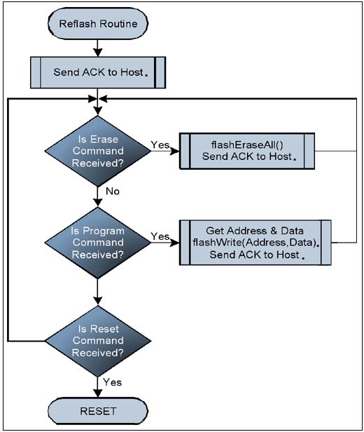
Figure 4. Flowchart of a simplified RAM reflash routine.
Appendix A. Code Examples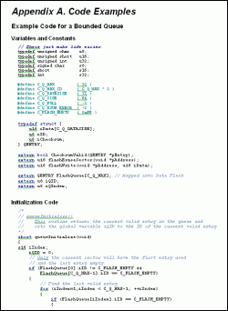
Download (DOC 53.5kB)
IntroducTIonThis application note describes how to manage the internal data and program flash in the MAXQ7665 flash-based microcontrollers (µC) with sector-erasable (SE) flash memory. This discussion includes general information for performing in-application programming (IAP) of the program flash.
Memory MapsThis section details the general flash information and memory organization for various memory sizes of the MAXQ7665 devices. There are two types of flash memory available on the MAX7665 devices. This document only covers the MAXQ7665 devices with SE flash and does not apply to the page -erasable (PE) devices. For information on MAXQ7665 PE devices, please refer to application note, "In-Application Programming (IAP) of the MAXQ7665 Page-Erasable (PE) Program and Data Flash".
Table 1 shows the flash memory maps for the 128KB, 64KB, 48KB, and 32KB devices. Other flash options may exist, so please consult the MAXQ7665 data sheet for a complete list.
Table 1. Flash Memory Maps
Using Flash to Store Data The flash can be used to reliably store system data that needs to be programmed once or periodically during system operation. While any sector of flash can be used to store data, the two 4K x 16 sectors usually provide the best fit. Unlike EEPROM, flash on the MAXQ7665 cannot be word erased. A complete sector must be erased at one time. Erasing a sector typically takes 0.7 seconds, but can take as long as 15 seconds under worst-case conditions. During this time the user code is stalled so no other processing can occur. These limitations must be considered carefully when you choose the software technique appropriate to your system requirements. For most periodic data-storage needs, a bounded queue and / or a bank switching technique will meet the reliability requirements and needs of the system. Simple examples of both techniques follow.
Bounded QueueA bounded queue is a queue limited by a fixed number of items. This technique is commonly used whenever periodic data is processed. For example, the 4K x 16 flash sector can be divided into 64 64-word entries, which would result in the memory map in Table 2 for the 128kB part.
Upon initialization, a startup routine can scan the queue entries to determine the next available entry in the queue. Once the queue is full, it must be erased before another entry can be written. (Note: if all entries are needed, then you must also use bank switching to maintain all the data.) Once the flash is erased, the new entry can be written. The drawback to this approach is that all data can be lost if there is a drop in power during the erasing process. If the bounded-queue technique does not meet the system's requirements, then bank switching will also be needed.
Figure 1 illustrates the flow of entries into a bounded queue.
See Appendix A for a simple C source-code example.
Table 2. Example of a Bounded-Queue Memory Map
| FLASHQueue [] | |
| Queue Index | Data Flash Address |
| 63 | 0xFFC0-0xFFFF |
| 62 | 0xFF80-0xFFBF |
| 61 | 0xFF40-0xFF7F |
| ... | ... |
| 2 | 0xF080-0xF0BF |
| 1 | 0xF040-0xF07F |
| 0 | 0xF000-0xF03F |
Figure 1. Bounded queue flow.
Bank SwitchingBank switching is an effective method of preventing data loss or corruption during the long sector-erase cycles. This method works well when the sector size is only slightly larger than the total data size. The drawback to bank switching is that it requires minimally two sectors of flash. When the total data size to be written is much smaller than the sector size, the best approach combines bank switching and bounded queue techniques. If bank switching is necessary for the application then, the two 4K x 16 flash sectors of the MAXQ7665 can be used as data storage.
Table 3 is an example of a memory map when using two 4K x 16 flash sectors. Figure 2 illustrates the bank-switching write / erase flow.
See Appendix A for a simple C source-code example.
Table 3. Example of a Bank-Switching Memory Map
| Flash Sectors | |
| Sector Number | Data Flash Address |
| 0 | 0xF000-0xFFFF |
| 1 | 0xE000-0xEFFF |
Figure 2. Bank switching flow.
Bounded Queue and Bank SwitchingUsing the bounded-queue and bank-switching techniques together is the most reliable and flexible approach. This combined approach works well when small amounts of data need to be stored to flash periodically, and when data integrity must be maintained. Table 4 shows an example of a memory map using the two 4K x 16 sectors divided into 64 equal entries. Figure 3 illustrates the flow of data in the bounded queue between the two sectors.
The coding for this combined technique is only slightly more complex than a bounded queue alone. See Appendix A for a simple C source-code example.
Table 4. Example of a Bounded-Queue Memory Map
| FQueueBank0 [] | |
| Queue Index | Data Flash Address |
| 63 | 0xFFC0-0xFFFF |
| 62 | 0xFF80-0xFFBF |
| 61 | 0xFF40-0xFF7F |
| ... | ... |
| 2 | 0xF080-0xF0BF |
| 1 | 0xF040-0xF07F |
| 0 | 0xF000-0xF03F |
| FQueueBank1 [] | |
| Queue Index | Data Flash Address |
| 63 | 0xEFC0-0xEFFF |
| 62 | 0xEF80-0xEFBF |
| 61 | 0xEF40-0xEF7F |
| ... | ... |
| 2 | 0xE080-0xE0BF |
| 1 | 0xE040-0xE07F |
| 0 | 0xE000-0xE03F |
Figure 3. Flowchart for bounded queue and bank switching.
Utility ROM Flash RoutinesTo program, erase, and verify flash, the MAXQ7665 microcontroller has on-chip flash-support routines residing in ROM (read-only memory). There are two ways to access these routines. The first and fastest method is direct access , that is to directly call the routine. To do this, provide a header file with the following lines:
u16 flashEraseSector (void *); u16 flashEraseAll (void); u16 flashWrite (void * pAddress, u16 iData); Next, add linker defines to assign the appropriate address for each routine. For the IAR linker file, the added lines would look like this:
-DflashEraseSector = 0x8XXX -DflashEraseAll = 0x8XXX -DflashWrite = 0x8XXX Replace 0x8XXX with the appropriate memory address for each routine. Other compilers might use a different method for adding these references.
Note: the direct-access method does not provide forward compatibility with future ROM versions.
The second method of indirect addressing uses a table lookup. While this method provides greater compatibility with future ROM versions, it consumes greater execution time. After each routine described below, an assembly routine uses the table-lookup method to obtain the address of the ROM Utility routine. Table 5 shows the flash routines supplied by the Utility ROM. For a complete listing of ROM Utility routines, please refer to the MAXQ7665 User's Guide which can be found o the Maxim website.
Table 5. Flash Utility ROM Routines
| Routine Number | Routine Name | Entry Point ROMTable = ROM [800Dh] | Entry Point Physical Address |
| 2 | flashEraseSector | ROM [ROMTable + 1] | 0x8XXX |
| 3 | flashEraseAll | ROM [ROMTable + 2] | 0x8XXX |
| 15 | flashWrite | ROM [ROMTable + 14] | 0x8XXX |
flashWrite
| Routine: | u16 flashWrite (void * pAddress, u16 iData) |
| Summary: | Programs a single word of flash memory. |
| Inputs: | A [0] —Word address in flash memory to which to write. A [1] —Word value to write to flash memory. |
| Outputs: | Carry: Set on error and cleared on success. If set, then A [0] contains one of the following error codes: 1: failure due to software timeout 2: failure reported by hardware (DQ5 / FERR) 4: command not supported SW_FERR—Set on error, cleared on success. |
| Notes: | The watchdog must not be active, or the watchdog timeout must be set long enough to complete this routine without triggering a reset. |
The following example of assembly code calls the flashWrite () utility routine using the indirect addressing method (lookup table). This routine is callable by C code.; This routine is callable by C code using the following prototype; u16 flashWrite (void * pAddress , u16 iData);; flashWrite: move APC, # 0; No auto inc / dec of accumulator. move DP [0], # 0800Dh; This is where the address of the table is; stored. move ACC, @DP [0 ]; Get the location of the routine table. Add # 14; Add the index to the flashWrite routine. Move DP [0], ACC move ACC, @DP [0]; Retrieve the address of the routine. Call ACC; Execute the routine. ret; Status returned in A [0]. flashEraseSector
| Routine: | u16 flashEraseSector (void * pAddress) |
| Summary: | Erases a single sector of flash memory. |
| Inputs: | A [0] —Address located in the sector to erase. |
| Outputs: | Carry: Set on error and cleared on success. If set, then A [0] contains one of the following error codes: 1: failure due to software timeout 2: failure reported by hardware (DQ5 / FERR) 4: command not supported SW_FERR—Set on error, cleared on success. |
| Notes: | |
| The watchdog must not be active, or the watchdog timeout must be set long enough to complete this routine without triggering a reset. |
; This routine is callable by C code using the following prototype; u16 flashEraseSector (void * pAddress);; flashEraseSector: move APC, # 0; No auto inc / dec of accumulator. Move DP [0], # 0800Dh; This is where the address of the table is; stored. move ACC, @DP [0]; Get the location of the routine table. add # 1; Add the index to the flashEraseSector routine. move DP [0], ACC move ACC, @DP [0]; Retrieve the address of the routine. Call ACC; Execute the routine. Ret; Status returned in A [0] flashEraseAll
| Routine: | void flashEraseAll (void) |
| Summary: | Erases the entire program and data flash memory, including the boot-loader sector. This routine is not normally used for IAP, as great care must be taken to insure that the erase / programming sequence is not interrupted. |
| Inputs: | None |
| Outputs: | Carry: Set on error and cleared on success. SW_FERR—Set on error, cleared on success. |
| Notes: | The watchdog must not be active, or the watchdog timeout must be set long enough to complete this routine without triggering a reset. |
; This routine is callable by C code using the following prototype; void flashEraseAll (void);; flashEraseAll: move APC, # 0; No auto inc / dec of accumulator. Move DP [0], # 0800Dh; This is where the address of the table is; stored. move ACC, @DP [0]; Get the location of the routine table. add # 2; Add the index to the flashEraseAll routine. move DP [0], ACC move ACC, @DP [0 ]; Retrieve the address of the routine. Call ACC; Execute the routine. Ret In-Application Programming (IAP) Most flash-based systems must have the ability to update firmware while the system is installed in the end product. This procedure is known as In-Application Programming (IAP). The following discussion outlines general guidelines for creating an IAP application.
The Utility ROM flash routines outlined in the previous section perform all the actions necessary to erase and write the flash ROM. It is, therefore, possible for an end-user application to perform operations on the flash memory. Like any other subroutine call, control will return to the end-user's code after completion of the routine.
Care must be taken when executing an IAP sequence on sector-erase-only versions of the MAXQ7665 since no dedicated boot-loader flash sector exists. To design a fully fault-tolerant IAP, the boot-loader application must be separate from the main application . This ensures that the reprogramming procedure can be retried even after an incomplete reprogramming sequence has occurred. If IAP must tolerate failures such as power loss during the reprogramming sequence, then select a MAXQ7665 version with page-erase capability. This will allow the boot- loader application to start at 0x0000 (the reset entry point), and be fully separate from the main application code. For applications that do not require a fully fault-tolerant IAP, then IAP can be accomplished using a RAM-based reflash routine.
IAP Using a RAM-Based Flash RoutineA RAM-based flash routine can be used to reflash the MAXQ7665 when fault recovery is not required. This method requires that the main application copy a small relocatable flash-programming routine into RAM and then jump to the routine . When executing code from RAM, there are several restrictions that must be considered.
Table 6. Restrictions When Executing Code from RAM
| SC.UPA must be set to 0 before executing a RAM-based routine. This means that the application must jump to the RAM routine from the code segments P0 and P1. |
| RAM cannot be accessed as data and program at the same time. This means that only the registers and hardware stack are available for data storage. |
| The Interrupt Vector must point to a RAM routine if interrupts are enabled. Typically interrupts are turned off and polling is used due to the simplicity of the RAM reflash routine. |
Typically, the flash routine will communicate through either the UART or CAN interface. It is usually best to receive small packets of data and send an acknowledgement to allow for a more robust error-recovery mechanism. Figure 4 is a flowchart showing how a reflash routine can work. If reprogramming is not successfully completed before loss of power, remember that the microcontroller will need to be reprogrammed through the JTAG port.
Figure 4. Flowchart of a simplified RAM reflash routine.
Appendix A. Code Examples
Download (DOC 53.5kB)
Mirror Heating Elements can be used in many field. Such as car rearview mirror.bathroom mirror.camera even in flower showcase freezer.With the property of automatically power change,the PET heating film can convert the electrical energy into thermal energy efficiently which makes the mirror suface's temperature rise to prevent steam from condensing. Not only did we supply the good quality of manufactured goods but also offer service of custom-made mirror heating film.We look forward to build business cooperation with customers worldwide.
Mirror Heating Elements
Rearview Mirror Heating Film,Ptc Heating Film , Mirror Heating Elements,Bathroom Mirror Heating Film
ShenZhen XingHongChang Electric CO., LTD. , https://www.xhc-heater.com