An AGC circuit with simple circuit and excellent performance
The AGC circuit of the receiver in the short-wave digital communication system is realized by the AD603 variable gain amplifier combined with a simple AGC control circuit. It has a high gain, a dynamic range of 70dB, a frequency bandwidth of 90MHz, and a relatively simple circuit structure.
When the shortwave receiver receives a signal, the signal level at its input varies within a wide range due to different ionospheric changes, fading, and received signal conditions. The output power of the receiver varies with the size of the external signal, and a very wide signal power will appear at the output of the receiver. For this reason, automatic gain control (AGC) circuits are very emphasized in short-wave receivers. The AGC circuit is an automatic control circuit that keeps the output signal amplitude constant or changes only in a small range when the input signal amplitude changes greatly. The basic principle of AGC is to generate a DC AGC voltage that changes with the input level, and use the AGC voltage to control the gain of certain amplification components (such as a central amplifier), so that the total gain of the receiver changes according to a certain rule. The AGC circuit is mainly composed of a control circuit and a controlled circuit. The control circuit is the generating part of the AGC DC voltage. The function of the controlled circuit is to change the gain of the receiver according to the changing control voltage generated by the control circuit.
At present, there are two main methods for controlling the gain of amplifiers in shortwave receivers. One is to change the parameters of the amplifier itself to change the gain. Typically, a double-gate field effect tube is used to change the gain by changing the DC bias voltage of one of the gates; the other is to insert a The variable attenuator controls the amount of attenuation to change the gain. Typically, various integrated variable gain amplifiers are used. The AGC circuit discussed in this article is implemented by using the AD603 variable gain amplifier of ADI and a simple AGC control circuit. The gain is required to be greater than 50dB, the AGC dynamic range is greater than 65dB, and the output signal level is basically stable at -10dBm.
Working principle of AD603

Table 1: AD603 pin functions
The AD603 is a low-noise, 90MHz bandwidth gain adjustable integrated op amp. If the gain is expressed in decibels, the gain is linearly related to the control voltage. The connection mode between the pins determines the programmable gain range, the bandwidth is 90MHz when the gain is -11 ~ + 30dB, and the 9MHz bandwidth is when the gain is +9 ~ + 41dB. Changing the connection resistance between the pins can make the gain Within the above range. The integrated circuit can be applied to radio frequency automatic gain amplifiers, video gain control, A / D conversion range expansion, and signal measurement systems. The simplified block diagram is shown in Figure 1.
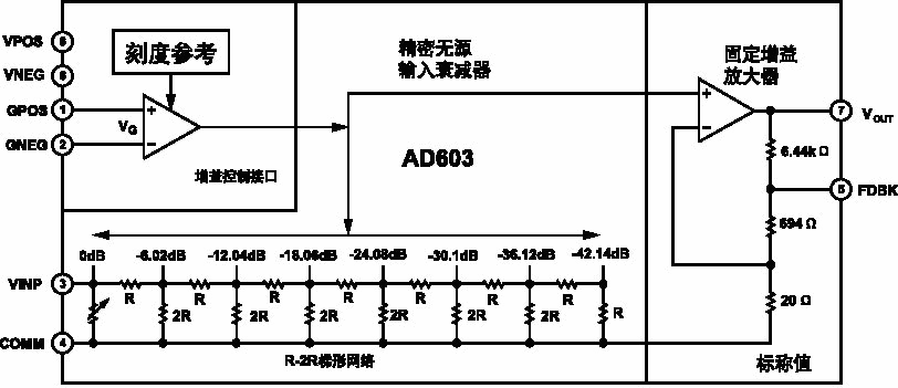
Figure 1: Functional block diagram of AD603
AD603 is composed of passive input attenuator, gain control interface and fixed gain amplifier. The signal added to the input terminal (VINP) of the ladder network in the figure is attenuated and then output by a fixed gain amplifier. The amount of attenuation is determined by the voltage applied to the gain control interface. Gain adjustment has nothing to do with its own voltage value, but only with its difference value VG. Since the input resistance of the control voltage GPOS / GNEG terminal is as high as 50MΩ, the input current is very small, so that the on-chip control circuit affects the external circuit that provides the gain control voltage small. The above characteristics are very suitable for constructing a program-controlled gain amplifier. The "sliding arm" in Figure 1 can be moved from left to right. When the connection between the two pins of VOUT and FDBK is different, the gain range of the amplifier is also different.
When pin 5 and pin 7 are short-circuited, the gain of AD603 is 40Vg + 10, and the gain range at this time is -10 ~ 30dB. This design is applied in this way. When pin 5 and pin 7 are disconnected, the gain is 40Vg + 30, and the gain range at this time is 10-50dB. If a resistor is connected to pins 5 and 7, the gain range will be between the two.
AGC circuit working principle and gain distribution and calculation
â— Working principle of AGC circuit
Choose AD603 as the main amplifier, two AD603 adopt the order cascade form, give full play to the gain control function of each AD603. AGC detection is completed by 9018, and 9018 sends out AGC control voltage at the same time. The complete amplifier and AGC circuit are shown in Figure 2.
The signal amplified by the two-stage AD603 is sent to the next-stage signal channel via J2, and the other is input from C10 to 9018 for AGC detection. The emitter PN junction of 9018 completes the AGC detection, and the collector sends the AGC control voltage VAGC after the capacitor CAGC is filtered.
When the input signal increases, the instantaneous base current of 9018 also increases, and the corresponding collector current also increases, so that the instantaneous voltage drop across R7 also increases, then the instantaneous collector voltage decreases. VAGC also decreases accordingly; similarly, when the input signal decreases, VAGC will increase, that is, VAGC is inversely proportional to the strength of the input signal, which meets the AGC voltage reverse control requirements.
Pin 2 of AD603 has a fixed voltage drop to ground, and the voltage drop of pin 1 to ground is VAGC, so the voltage difference V12 between pin 1 and pin 2 is controlled by VAGC. The gain of AD603 can be expressed as: G = 40 · V12 + 10. It can be seen that as VAGC increases, V12 also increases, the gain of AD603 becomes larger; on the contrary, if VAGC decreases, V12 also decreases, the gain of AD603 becomes smaller, so that the output of the two-stage AD603 is constant at a certain level Signal strength. The adjustment of the AGC time constant can be achieved by changing the capacitance of CAGC.
â— AGC gain allocation and calculation
The two AD603 adopts the sequential cascade mode, which is conducive to the improvement of control accuracy and signal-to-noise ratio. The sequential cascade mode requires that the gain of the first chip AD603 be enabled when the signal is amplified, and then the gain of the second chip is used after it is exhausted. According to the gain calculation formula of AD603, when V12 is between -500 ~ 500mV, its gain changes within the range of -10 ~ 30dB, then there should be a voltage difference of 1V between V12 of the two AD603, reflected in Figure 2. , That is, there is a voltage drop of 1V between the two feet of AD603.

Figure 2: Amplifier and AGC circuit
According to the actual design, a certain margin should be left. The gain range of the first AD603 is set to -6 ~ 30dB, the corresponding V12 is -400 ~ 500mV, and its 2 feet have been fixed at 5.5V, so the control voltage of 1 foot, VAGC, should be 5.1 ~ 6V. The gain range of the second AD603 is set to -10 ~ 24dB, then the corresponding V12 is -500 ~ 350mV, and its 2 pin has been fixed at 6.5V, so the control voltage of 1 pin, VAGC, should be 6 ~ 6.85V The total gain range after the chip is cascaded sequentially is -16 ~ 54dB, as shown in Figure 3.
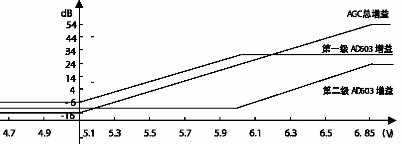
Figure 3: AGC gain allocation
From the above analysis, when the AGC control voltage VAGC changes from 5.1V to 6.85V, the total gain of the two-stage AD603 will increase linearly from -16dB to 54dB. What needs to be done now is to adjust the working point of 9018 so that when the input signal changes appropriately, the AGC control voltage VAGC varying from 5.1V to 6.85V can be taken from the collector of 9018. As can be seen from Figure 2, the size of VAGC depends on the resistance of R7 and the size of the collector current.
When there is no signal input, adjust the static working point of 9018 so that the PN junction of the 9018 emitter is at an approximate cut-off state, and adjust the resistance of R7 so ​​that the VAGC is 6.85V. At this time, the gain of the two stages AD603 is all released, that is, 54dB ; When there is a signal input, but the signal strength cannot yet turn on the PN junction of the 9018 emitter, the AGC is out of control, and the output signal will increase as the input signal strength increases; when the signal strength is enough to make the 9018 launch When the PN junction of the pole is turned on, the 9018 is in the AGC detection state. At this time, the AGC starts to control, and the VAGC decreases at a rate of about 25mV / dB until it drops to 5.1V. The gain of the corresponding two-stage AD603 also gradually decreased from 54dB to -16dB. First, the gain of the second-stage AD603 gradually decreased from 24dB to -10dB, and then the gain of the first-stage AD603 also gradually decreased from 30dB to -6dB. At this point, AGC enters the saturation point, when the input signal strength increases again, AGC has lost control, and the output signal will increase as the input signal strength increases. This is the entire control process of AGC, that is, as the input signal strength continues to increase, AGC will go through the control process of running out of control, starting control, entering saturation, and running out of control again.
â— Selection and calculation of AGC starting point and saturation point
The selection of AGC starting point and saturation point should be calculated according to the specific application. Assuming that the required signal is amplified by AGC, its signal strength is stable at W (dBm), and the AGC gain range is Ga ~ Gb (dB), then the AGC starting control point level (dBm) is W-Gb; AGC saturation point level ( dBm) is W-Ga. In application, after the signal is amplified by two stages AD603, the signal strength is basically stable at -10dBm, and the AGC gain range is -16 ~ 54dB, so the AGC starting control point level should be -10-54 = -64 ( dBm); AGC saturation point level should be -10-(-16) = 6 (dBm). Therefore, the dynamic range of the signal that AGC can process is -64 ~ 6dBm, a total of 70dB.
The adjustment of AGC starting point can be achieved by changing the resistance of R5. In fact, changing the resistance of R5 is to adjust the PN junction voltage drop of the 9018 emitter. When this PN junction is used for AGC detection, its voltage drop is biased between 500 and 700mV. Assuming that the instantaneous voltage drop of this PN junction during operation is 600mV, AGC starts to control, and assuming that the required AGC starting point level is -30dBm (20mV), then, by adjusting the resistance of R5, this PN The junction is biased at 580mV, when the input signal level reaches 20mV, the instantaneous voltage drop of this PN junction is 600mV, and the AGC starts to control. The above is only a qualitative approximate analysis. In the actual circuit implementation, it is necessary to repeatedly adjust the resistance of R5 according to the measurement results to meet the requirements of the AGC starting point. Of course, the AGC starting point has a lower limit. As far as the AGC control circuit shown in FIG. 2 is concerned, the lower limit of its AGC control depends on the adjustment accuracy of the voltage drop of the PN junction of the 9018 emitter. After actual measurement, this value is about 100 μV (-76 dBm).
Experimental data
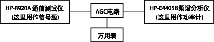
Figure 4: AGC test block diagram
Connect the entire circuit as shown in Figure 4 for a closed-loop test. During the test, the input signal strength was changed by adjusting the variable attenuator of HP-8920A. The output signal strength was observed by HP-E4405B. At the same time, the voltage value of VAGC was tested by a multimeter. The test data is shown in Table 2.

Table 2: AGC test data
It can be seen from the test data in Table 2 that when the input signal strength changes from -64 dBm to 6 dBm, the AGC control circuit can adjust the AGC control voltage VAGC accordingly, thereby changing the gain of AD603 so that its output signal strength is basically stable at- 10dBm, the entire control range is above 70dB, which meets the design requirements.
Product categories of Tealight Candle, we are specialized manufacturers from China, Tealight Candle, 10G Color Tealight Candle suppliers/factory, wholesale high-quality products of 12G Poured White Tealight Candle and manufacturing, we have the perfect after-sales service and technical support. Look forward to your cooperation!
12 Gram Tealight Candle,Tealight Candles For Party,Long Burning Tealight Candle,Scented Tealight Candles
Shijiazhuang Zhongya Candle Co,. Ltd. , https://www.zycandlefactory.com